EE466/EE966/EE875 Coursework Assessment Part 2: Power Electronics Section
Hello, dear friend, you can consult us at any time if you have any questions, add WeChat: daixieit
EE466/EE966/EE875 Coursework Assessment Part 2:
Power Electronics Section
Introduction
The objective of this coursework exercise is to consolidate the lecture material that you have received, and to bring together associated engineering topics that relate to the analysis and design of power electronic circuitry.
Another important objective is to assist you in the development of transferable skills, such as report writing, presentation of technical material, and examination technique.
The Assessment
The assessment consists of three questions where all of the material has been covered to greater or lesser degrees during lectures. All questions should be answered for maximummarks, and be careful to ensure you have attempted all parts of each question. Whilst some questions are straightforward, others are designed to test your comprehension beyond what has been explicitly covered in the class.
Submission
• You must submit a computer-processed report with the solutions.
• Your submission must include a cover sheet (free format).
• When including your name on the cover sheet, it must be presented in the order:
First Name Family Name
• If your solutions require graph solutions, you should include the plots in the report.
• Your solutions should resemble ‘specimen solutions’, i.e. the type of solution that you may expect to see in a textbook. Solutions must be clearly presented, legible, and concise. You should show all of your mathematical working. Diagrams and graphs must be clear and contain all of the relevant information.
• In order to answer some of the questions, it will be necessary to consult background material. We expect the student to use resources like IEEE Explore, IET library, Elsevier library or the University library instead of Wikipedia. A list of references should be added to the coursework where appropriate.
• Students should take responsibility for observing the university regulations on plagiarism.
• Your completed assessment must be submitted online by 12 noon on Monday 18 March.
• YOUR UPLOADED DOCUMENT MUST BE IN PDF FORMAT.
QUESTION 1
Q1 An IGBT and a diode forming a power converter are mounted onto a
heatsink. Thermal data for this arrangement are given in Table Q1. The ambient temperature Tamb is 40°C.
Table Q1.
|
IGBT |
Power dissipation WIGBT in IGBT |
12 W |
|
Junction to case thermal resistance Rθjc |
0.6°C/W |
|
|
Case to heatsink thermal resistance Rθchs |
1.4°C/W |
|
|
|
|
|
|
Diode |
Power dissipation WDIODE in diode |
7 W |
|
Junction to case thermal resistance Rθjc |
0.9°C/W |
|
|
Case to heatsink thermal resistance Rθchs |
1.5°C/W |
|
|
|
|
|
|
Heatsink |
Heatsink to ambient thermal resistance Rθhsa |
3.2°C/W |
|
Thermal capacitance Cθhs of heatsink |
280 J/°C |
Q1a i. Sketch a clearly-labeled thermal circuit.
ii. Calculate the steady-state temperature of the diode and IGBT junctions.
iii. Calculate the heatsink’s temperature three minutes after the circuit is de-energised after it has been running in the thermal steady-state.
13 marks
Q1b You have designed a buck converter, and as part of the design validation
programme you need to experimentally measure the converter’s switching
losses. Thermal superposition measurements or double-pulse testing can be
used for this. Describe how these techniques work, and discuss their advantages and limitations.
12 marks
QUESTION 2
Q2a i. Transformers in switched-mode power converters often use ferrite
core materials. Alternatively, nanocrystalline materials can be used in this application. Discuss the relative merits and demerits of ferrite
and nanocrystalline core materials when used in a power converter’s transformer.
ii. Chokes in switched-mode power converters often also use ferrite core materials. Alternatively, iron powder materials can be used in this application. Discuss the relative merits and demerits of ferrite and iron powder core materials when used in a power converter’s choke.
8 marks
Q2b Figure Q2b shows a rectifier circuit using a thyristor. The AC supply voltage
vac is 230 V, and RLOAD has a resistance of 500 Ω. Calculate the average value of iLOAD if the thyristor is triggered at an angle α of 65° .
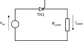
Figure Q2b. Rectifier circuit.
7 marks
Q2c A MOSFET is mounted onto a heatsink, and data for this arrangement are
given in Table Q2(c). The MOSFET switches at a very low frequency and hence its switching losses can be neglected, and the only significant losses are its conduction losses. Calculate the MOSFET’s junction temperature.
Table Q2(c). Data for MOSFET mounted on heatsink.
|
Ambient temperature |
Tamb |
20°C |
|
MOSFET’s RDS(on) when at 20°C |
RDS(on)20 |
25 mΩ |
|
RMS current conducted by MOSFET |
Irms |
16 A |
|
Total thermal resistance between MOSFET junction and ambient |
Rθ |
7°C/W |
|
Coefficient of rise in RDS(on) with temperature |
kθ |
1.1%/°C |
When answering this question, consider that a positive feedback mechanism must be present because:
• The power dissipation in the MOSFET causes a rise in its junction temperature and;
• The rise injunction temperature increases the MOSFET’s RDS(on),thereby causing its power dissipation to increase.
In your answer it is suggested that you sketch a block diagram with the variables in Table Q2(c) interconnected, and use simple feedback controltheory to calculate the temperature.
10 marks
QUESTION 3
Q3 Figure Q3(a) shows a dual-switch forward converter. The input voltage Vin is 48 V, and the output voltage Vout is 14 V. Other data are given in
Table Q3(a).
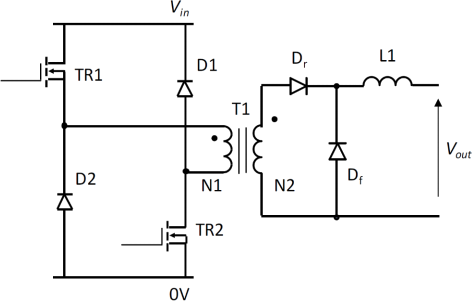
Figure Q3(a). Dual-switch forward converter.
Table Q3(a). Data for circuit in Figure Q3(a).
|
Full-load output power |
50 |
W |
|
Switching frequency |
120 |
kHz |
|
L1 inductance |
180 |
µH |
|
Transformer T1 turns-numbers N1:N2 |
32:26 |
- |
The transformer is constructed around EFD30 ferrite half-cores in 3C90
material. The manufacturer’s data sheet should be consulted to obtain data:
http://ferroxcube.home.pl/prod/assets/efd30.pdf
Q3a Calculate the following quantities:
i. the duty factor at which the converter operates when it is running in the continuous current mode;
ii. the minimum voltage that diode Dr must be able to support;
iii. the output power at which the converter will enter the boundary conduction mode;
iv. the flux density swing in the transformer’s core material;
v. the peak magnetizing current drawn by the transformer.
10 marks
Q3b TR1 and TR2 in Figure Q3(a) are normally driven on simultaneously by
applying a positive gate-source voltage to each of them. As seen in
Figure Q3(b), driving the lower device, TR2, directly from a low-voltage control IC connected to 0 V is relatively straightforward.
However, there is a difficulty with driving the upper device, TR1, as its source voltage swings between 0 V and 48 V. TR1 therefore cannot be driven directly from the output terminal of a low-voltage control IC connectedto 0 V.
With the aid of sketches, explain how circuitry using a bootstrap diode, flying capacitor, high-voltage level-shifting MOSFET and a driver IC can be incorporated to enable TR1 to be driven from the low-voltage control circuitry.
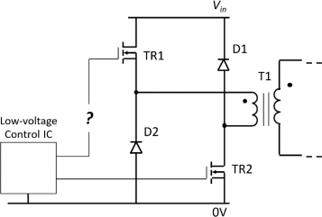
Figure Q3(b). Primary side circuitry of dual-switch forward converter in Figure Q3(a).
8 marks
Q3c Redraw the circuit in Figure Q3(a), but with the arrangement formed by Dr and
Df replaced with an arrangement of MOSFETs acting as synchronous
rectifiers. Explain what the benefits of this latter arrangement are, and how it operates. Sketch waveforms in your answer as appropriate.
7 marks
2024-03-05