Logic Block Design
Hello, dear friend, you can consult us at any time if you have any questions, add WeChat: daixieit
1 Logic Block Design
In this task, you are supposed to design some basic logic blocks in Verilog. Then you will verify your designs to see if they are working as expected. For each block, you should create a new project, write down the code in Verilog, and run the simulation. Below, you see each block description. We put the whole process of simulation for the first block here. You should follow the same process for the rest.
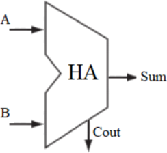
1.1 Half Adder
Design a Half Adder (HA) using Verilog logical operators. As you know, the Half Adder has 2 inputs and 2 outputs. Here is the block diagram for a Half Adder.
This is the truth table for a Half Adder:
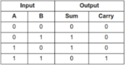
As you see, the Boolean equation for the two outputs (Sum and Cout) are as follow:
• Sum = A XOR B
• Cout = A AND B
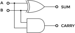
This is the circuit schematic for Half Adder:
Follow these steps to design and simulate a Half Adder in the Vivado:
• Create a new RT L project in the Vivado.
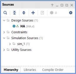
• Add a design source and choose Create File. Make sure to change the file type to Verilog. You can skip the I/O port definition (you will manually define the I/O ports by commands in your code). Your new source (.v) should now be under the Design Sources in the Sources window.
• Double click on it and enlarge the window. Write the code below and save the file.
Code 1: Half Adder.
‘timescale 1ns / 1ps // time - unit = 1 ns , precision = 1 ps
// Define the module
module HA(
A,
B,
Sum ,
Cout
);
// Define the input and output signals
input A;
input B;
output Sum ;
output Cout ;
// Define the modules behavior
assign Cout = A & B; // bitwise and
assign Sum = A ˆ B; // bitwise xor
endmodule // HA
• Now to test the functionality of our design, we need to write a testbench. Create a new Simulation Source and write the code below.
Code 2: Half Adder Test Bench.
‘timescale 1ns / 1ps // time - unit = 1 ns , precision = 1 ps
module HA_tb ();
// Define the input and output ports
reg A_tb = 0;
reg B_tb = 0;
wire Sum_tb ;
wire Cout_tb ;
// Port Mapping
HA instant
(
.A( A_tb ),
.B( B_tb ),
.Sum ( Sum_tb ),
. Cout ( Cout_tb )
);
// Test samples
initial // initial block executes only once
begin
A_tb = 1’b0;
B_tb = 1’b0;
#10; // wait for 10 time - units (10 ns in this example )
A_tb = 1’b0;
B_tb = 1’b1;
#10; // wait for 10 time - units (10 ns in this example )
end
endmodule // HA_tb
• Save the code and run the simulation. To simulate the HA tb, right click on it and click “Set as Top”, then Run the Simulation.
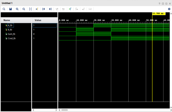
• Check the waveform. From time 0 to 10ns, the inputs are as follows: A=0, B=0, and the outputs are Sum=0 and Carry=0 as expected. For the next 10ns of the simulation, we have A=0, B=1, and the outputs are Sum=1 and Cout=0. Add some more tests to the test bench code and see the result on the waveform. P u t a screenshot for the waveform for 2 more test cases with their explanation in your report.
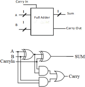
1.2 1-bit Full Adder
Now try to design a 1-bit Full Adder using Verilog logical operators. Below you see the diagram and the circuit schematic for a 1-bit Full Adder.
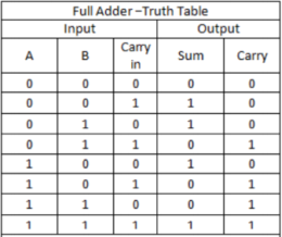
This is the truth table for 1-bit Full Adder:
As you see the Boolean equation for the two outputs (Sum and Cout) are as follow:
• Sum = A XOR B XOR Cin
• Cout = (A AND B) OR (A AND Cin) OR (B AND Cin)
Start coding for 1-bit Full Adder using Verilog logical operators. Define signals and complete the module behavior.
Code 3: 1-bit Full Adder.
‘timescale 1ns / 1ps
// Module definition
module FA(
A,
B,
Cin ,
Sum ,
Cout
);
// Define the input and output signals
// Define the full adder modules behavior
endmodule // FA
Simulate your code. Write a test bench for your design and run the tests below.
Test1 ( R u n for 20ns): A=‘0’ , B = ‘1’, Cin = ‘0’
Test2 ( R u n for 20ns): A=‘1’ , B = ‘1’, Cin = ‘0’
Test3 ( R u n for 20ns): A=‘1’ , B = ‘1’, Cin = ‘1’
1.3 4-bit Full Adder
Design a 4-bit Full Adder using Verilog logical operators. Below, you see the block diagram for a 4-bit Full Adder.
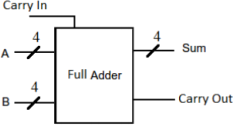
This is the circuit schematic for a 4-bit Full Adder. Blue lines inside the box are not connected to any input or output ports. We need to define them in the code as a SIGNAL .
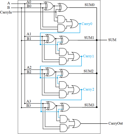
Define signals, complete the code and run the simulation. Write a testbench for your design and run the tests below.
Test1 ( R u n for 20ns): A=“0110” , B = “0100”, Cin = ‘0’
Test2 ( R u n for 20ns): A=“1000” , B = “1001”, Cin = ‘1’
Test3 ( R u n for 20ns): A=“1110” , B = “0010”, Cin = ‘0’
Test4 ( R u n for 20ns): A=“1010” , B = “1011”, Cin = ‘0’
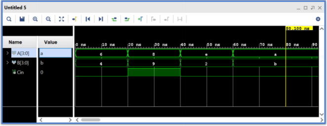
Check the outputs (Sum and Cout) to see if they are correct. P u t a screenshot of the wave in your report. Yo u r screenshot should look like this and includes the Sum and Cout signals.
Code 4: 4-bit Full Adder.
‘timescale 1ns / 1ps
// Module definition
module FA4 (
A,
B,
Cin ,
Sum ,
Cout
);
// Define the input and output signals
// Define the full adder modules behaviour
endmodule // FA4
1.4 Multiplexer 2:1
Design a 1-bit, 2 to 1 multiplexer using Verilog logical operators. You should have a select input to be able to choose from two 1-bit inputs. This is the block diagram for the 2:1 multiplexer.
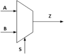
In particular, when S is ‘0’, the output is A, when S is ‘1’, the output is B
Use this sample code for your module declaration.
Code 5: Multiplexer 2 to 1.
‘timescale 1ns / 1ps
// Module definition
module Mux_2_To_1 (
input S,
input D1 ,
input D2 ,
output Y);
// Define the MUX2 :1 module behaviour
endmodule // MUX2 :1
Write a testbench for your design and run the tests below.
test1 ( R u n for 20ns): D1=‘0’ , D2 = ‘1’, S = “0”
test2 ( R u n for 20ns): D1=‘0’ , D2 = ‘1’, S = “1”
Check the output ( Y ) to see if it is correct. P u t a screenshot of the wave in your report.
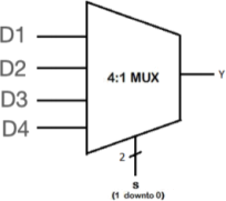
1.5 Multiplexer 4:1
Design a 1-bit, 4 to 1 multiplexer using Verilog logical operators. You should have a 2-bit select input to choose from four 1-bit inputs. Here you see the block diagram for 4:1 multiplexer.
Use this sample code for your module declaration.
Code 6: Multiplexer 4 to 1.
‘timescale 1ns / 1ps
// Module definition
module Mux_4_To_1 (
input [1:0] S,
input D1 ,
input D2 ,
input D3 ,
input D4 ,
output Y);
// Define the MUX4 :1 modules behavior
endmodule // MUX4 :1
Write a testbench for your design and run the tests below.
Test1 ( R u n for 20ns): D1=‘0’ , D2 = ‘1’, D3=‘0’ , D4 = ‘1’, S = “00”
Test2 ( R u n for 20ns): D1=‘0’ , D2 = ‘1’, D3=‘0’ , D4 = ‘1’, S = “01”
Test3 ( R u n for 20ns): D1=‘0’ , D2 = ‘1’, D3=‘0’ , D4 = ‘1’, S = “10”
Test4 ( R u n for 20ns): D1=‘0’ , D2 = ‘1’, D3=‘0’ , D4 = ‘1’, S = “11”
Check the output ( Y ) to see if it is correct. P u t a screenshot of the wave in your report.
2. Deliverables
Your submission is on should include the following items:
• Module designs and testbenches. (FA.v , tb FA.v , FA4.v, tb FA4.v, mux21.v, tb mux21.v, mux41.v, tb mux41.v) (Remember: In Verilog the file name does not have to be the same as the module name.)
2024-01-24
Computer engineering