EN3082 Coursework 2: Transistor Matching
Hello, dear friend, you can consult us at any time if you have any questions, add WeChat: daixieit
EN3082 Coursework 2: Transistor Matching
This coursework involves the following:
. Using the impedance and admittance Smith chart (both ADS-based and paper-based)
. Using some key ADS tools – specifically LineCalc and the Smith Chart Tool.
. Use of s-parameters / reflection coefficient in understanding of impedance transformation.
. Lumped element matching and distributed element matching.
. A comparison of different types of bias networks used with power transistors
This coursework will make up 20% of the overall EN3082/ENT782 module mark. It will be set in week 7 and needs to be submitted by 12 midnight on Friday, week 11 of the Autumn Semester.
Design Brief: This coursework is in two parts. In the first part, you are required to consider the damaged transmission line you will design in Dan’s Coursework (also issued in week 7), in terms of the complex impedance it presents when attached directly to an active device.
In the second part, you will consider the properties of an active device, and will need to design various impedance transforming networks to match both the output and input of an actual, state-of-the-art, 10 Watt Gallium Nitride (GaN) power transistor, to 50 Ohm source and load impedances.
1 – Characterising the impedance presented by a damaged transmission line (5 marks)
1.1 Use ADS components to represent the transmission line with discontinuities (refer to Part I of Dan’s coursework) in ADS and extract the resulting S-parameter over a frequency range 1 to 20 GHz.
From Dan’s coursework: The model describes a 3.3mm wide, 50 Ω microstrip line on a 60 mil (60 mil is 1.524mm) substrate with the dielectric constant of εr = 3.38, and 65mm in length. Later, we will introduce two notches in the middle of the microstrip line to represent an impedance mismatch caused by physical damage, leading to unwanted signal reflections.
Using an ADS Schematic window, add an MSUB and MLIN components from the Microstrip Line pallet, and represent the transmission line with discontinuities as best you can. Note that you will not be able to exactly represent the discontinuities (that exist on only one side of the transmission line) as the ADS representation will need to be symmetrical about the horizontal axis, but this is OK.
Simulate the 2-port network over a wide bandwidth (1-20 GHz) and examine all four s- parameters. Plot S11 on a Smith chart and S21 on a log-linear plot, using appropriate titles, noting what you observe about how the two plots and how they relate. Use data display markers to clearly show any points of interest.
[5]
2 – Matching an active device (15 marks)
Gallium Nitride (GaN) transistors offer many advantages in power amplifier design. They can operate at higher frequencies, higher supply voltages and can offer higher output power and efficiency in comparison to other competing technologies such as GaAs and Si-LDMOS. This part of the coursework focuses on a specific device: the CGH40010, 10 W packaged device manufactured by Cree/Wolfspeed. Please use the datasheet supplied for the necessary design information. The fundamental design frequency is 2.45 GHz.
2.1 Your first job is to match the input of the device, using a cost-effective combination of a series transmission line and shunt capacitance. Then move onto matching the output of the device using the following three approaches:
a) lumped element components
b) distributed - 50 using only Ohm sections of transmission line
c) a series ¼ transmission line together with either lumped element or a distributed approach.
Use VERY clearly annotated paper Smith charts for your designs and use ADS only as a means of checking what you have done. Make sure to use the Smith chart in both admittance and impedance orientations, as discussed in lectures.
You will need the optimum source and load impedances ZS and ZL – these have already been measured for you, and are given on page 7 of the transistor’s data sheet. When using ADS, use TERM components to model these complex optimum impedances (use the conjugate ZS and ZL), allowing you to progress with the matching circuit design without needing the foundry device model. You will need to use a sensible method of interpolation to obtain these impedances at the fundamental frequency of interest (2.45 GHz). Use ADS to compare and contrast your output match
[10]
2.2 Optional - Introduce suitable biasing networks to both input and output matching circuits - use shorted ¼ wave transformers to achieve this. Again, use ADS to demonstrate that the biasing networks will not impact performance at the fundamental frequency.
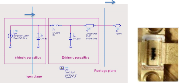
2.3 The output of this GaN device can be modelled as a current generator (Igen) followed by some intrinsic output capacitance Cds (2.5pF), and then extrinsic package parasitic components Lbond (2.5 nH), Cpad (0.5 pF) and TL1 (10 degrees @ 2.45 GHz) , as shown in the figure below. We are usually interested in impedances at two different ‘reference planes’ :
a) the current generator (Igen) plane (this exists intrinsically, within the device)
b) the package plane (where the metal tab of the transistor physically enters the package).
In high-performance amplifier design, for example when designing to achieve high- efficiency operation, we often start with a precise understanding of the specific impedances we need to present to the current generator within the device, at fundamental and harmonic frequencies (Fo , 2Fo and 3Fo).
For this device, the current generator needs to ‘see’ an optimum 40 Ohm real impedance at the fundamental frequency. Assuming a fundamental operating frequency of 1 GHz, use a paper Smith chart to determine the fundamental impedance that must be present to the device at the package plane.
[5]
2.4 Optional -The ‘class-F’ amplifier mode is an example of a high efficiency configuration. To achieve this mode using this GaN device used here, the current generator needs to see a short circuit at the 2nd harmonic frequency and an open circuit at the 3rd harmonic frequency. Higher harmonics can be ignored. Use a Smith chart to determine the second harmonic impedances that must be present at the package plane for this high-efficiency mode to exist for a fundamental frequency of 1 GHz (you can ignore the 3rd harmonic in your answer)
2024-01-12