Computer Hardware and Digital Design Assessed assignment Part 1
Hello, dear friend, you can consult us at any time if you have any questions, add WeChat: daixieit
Computer Hardware and Digital Design
Assessed assignment
Part 1
Introduction
The assignment will last for up to eight lab sessions. During the assignment you will design part of the core of a RISC microprocessor, and demonstrate it working. The assessment will be based on a report that you submit in January.
In part 1 of the assignment you will design the two main building blocks that will be used for this assignment: an ALU and a memory to hold data. In units 1.5 and 2.5 you can find basic templates and testbenches for an ALU and a memory that you will need to adapt to your requirements. This part of the assignment should take about 2 weeks to complete.
In part 2 of the assignment you will extend your data memory to hold the values of variables that your program is processing. Then you will connect the ALU and memory file together, and run a machine instruction on them. This part of the assignment should take one to two weeks.
In part 3 of the assignment you will resolve problems with the synchronisation of the instructions to ensure that a stream of machine instructions can run correctly. This part of the assignment should take the remainder of the lab sessions.
In order to ensure that your design is individual to you, various aspects of the design will be dictated by your student ID number. These include the machine code used by your design, the contents of the register file, and the purpose of the program that you will use to demonstrate the correctness of your design. This means that every student should have a unique design.
You may work as an individual or as a pair in labs, but each student will have to demonstrate their own individual design.
The ALU
Write a VHDL description of an ALU with two 32-bit inputs, A and B, and a 32-bit output Result.
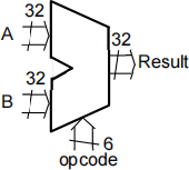
The result is derived from one or both of the inputs according to the value of a 6-bit opcode. The operations that the ALU can perform are listed below:
a + b
a - b
|a| (i.e. the absolute value of a: this is achieved using the VHDL function abs(a) )
-a
|b| (i.e. the absolute value of b)
-b
a or b
not a
not b
a and b
a xor b
The opcode that will be used to represent each of these operations is determined by the last digit of your student ID number. The table below shows which opcode you should use in your design for each instruction.
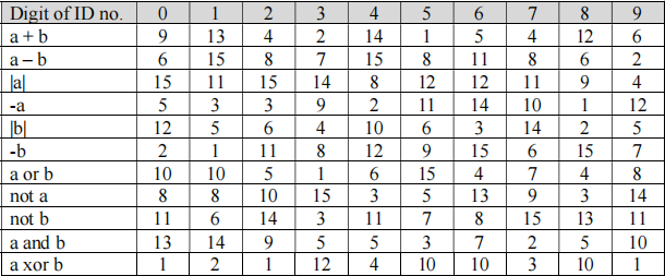
So, for example, if the last digit of your ID number is 2, then a+b is to be represented by opcode 4, a-b is to be represented by opcode 8, |a| is to be represented by opcode 15 and so on. (These are shown as denary values; your design will of course have to use binary or hexadecimal values.)
If the ALU receives an unrecognised opcode then it should output zero.
Create a testbench to show the correct operation of your ALU with a variety of test input conditions.
The data memory
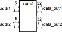
Inside a modern processor there is a very small amount of memory that is used to hold the operands that it is presently working on. This is called the register file. In order to introduce the operation of the register file, we will start off by building a small memory whose purpose is to hold the data that a program works on. It will have the following appearance:
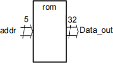
The ROM contains 32 data locations that each hold a 32-bit data word. These are addressed by a 5-bit input called addr. The data value stored at the location addressed by the addr input appears at the output called data_out.
The initial data values stored in the memory are determined by the second-from-last digit of your student ID, and are shown in the table below:
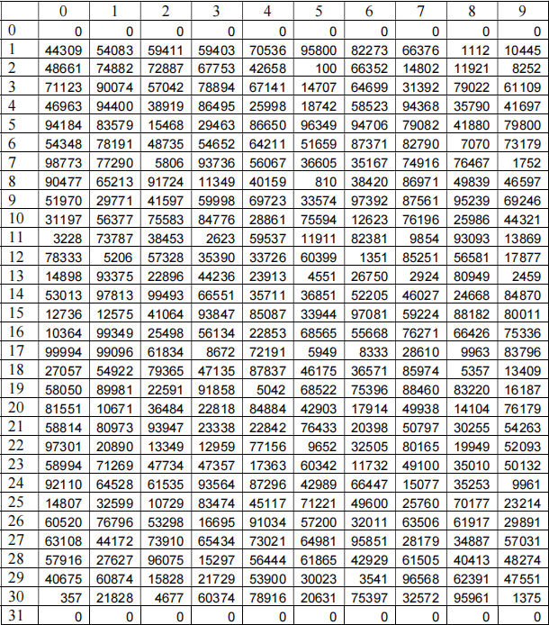
So, for example, if your student ID is 714583 then the second-from-last digit of your ID number is 8; so items 0 should be 0, item 1 should be 1112, item 1 should be 11921, and so on. N.B. these values are in denary (i.e. base 10). You will need to convert them to binary or hexadecimal.
If you need the above data in spreadsheet form, you can download it from the assignment section of the Canvas pages in the spreadsheet CHDDdata.xls. You may find the excel function dec2hex helpful in doing the conversions.
Create a testbench to show the correct operation of the ROM.
A two-port data memory
Now modify your ROM to create a dual ported ROM. This has two address inputs and two data outputs associated with the one set of data items stored in the ROM. The data value addressed by addr1 appears at the output data_out1 and the value addressed by addr2 appears at the output data_out2.
Connecting to the ALU
Now create a new VHDL file called micro. Use this to integrate the ALU and the memory together as shown below.
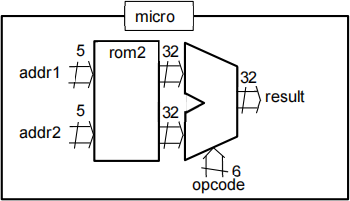
This arrangement can be used to perform arithmetic operations on the data values stored in the memory. For example, to add item 5 and item 6 you would supply the inputs addr1=5, addr2=6 and use the opcode value corresponding to add. The outcome of the computation will appear at the result output.
Use simulations to check out that your design works as expected.
2024-01-11