ECE 6463: Advanced Hardware Design 2022
Hello, dear friend, you can consult us at any time if you have any questions, add WeChat: daixieit
ECE 6463: Advanced Hardware Design 2022
Final EXAM (20% + 2%) IN-CLASS: December 16th 2022, 2:05-4:35 PM EDT
Instructions
● Read and complete all questions carefully.
● This exam is to be completed individually. Collaboration/plagiarism will not be tolerated.
● Please sign the code of conduct (located at the bottom of this exam) and include it in your submission.
● Do not use the internet for anything other than connecting to the “hansolo” server or as otherwise cleared with your examiner.
● You may examine your own notes from class and the class slides.
● Clarification questions can be asked to a member of the teaching team. Do not connect to the class slack during the exam.
● During the exam period, you will not be allowed to receive assistance from the teaching staff regarding the use of the tools or implementation/simulation.
OVERVIEW: In this examination you will design, implement, and simulate digital hardware with sequential and combinational logic to implement the control system for a one-lane railway bridge. This algorithm will be implemented in either the Verilog or VHDL languages. This is an example of a safety-critical application.
The system diagram is presented here:
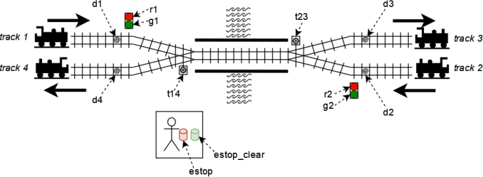
As can be seen, the system has the following essential properties:
1. Tracks 1-4 are one-way train tracks. The bridge is a two-way train track (it is a shared resource).
2. Trains that enter on Track 1 will leave on Track 3. Trains that enter on Track 2 will leave on Track 4.
3. A Train will enter the bridge if the appropriate signal light is green (g1/g2 == 1). It will stop if the appropriate signal light is red (r1/r2 == 1). There should be no circumstance where a given signal has both red and green illuminated simultaneously, nor any circumstance where a signal has no light illuminated.
4. A train requests passage on the bridge by reaching the appropriate entry detector (d1/d2). That is, if d1 == 1, a train is waiting on Track 1 to cross the bridge. If d2 == 1, a train is likewise waiting on Track 2.
5. Track switches t14 and t23 choose which tracks are connected to the bridge.
a. If t14 == 1, the bridge is joined to Track 1.
b. If t14 == 0, the bridge is joined to Track 4.
c. If t23 == 1, the bridge is joined to Track 2.
d. If t23 == 0, the bridge is joined to Track 3.
6. After granting a train access to the bridge, no track switch changes should occur. Also, no other train should be granted access to the bridge until the granted train is clear.
7. To detect if a train is clear, it should “pass over” the appropriate exit detector (d3/d4). That is, simply reaching the detector (d3 == 1 or d4 == 1) does not imply the train has exited - that means the train has reached it. The train has exited once the detector returns to the 0 value. In other words, a 1 followed by a 0 on the exit detector equals a train exit.
8. As a complete ‘passage ’ example:
a. The bridge is empty → r1 == 1, r2 == 1, g1 == 0, g2 == 0
b. A train arrives on Track 1 → d 1 == 1
c. The junctions are set appropriately for a Track 1 passage → t14 == 1, t23 == 0
d. The appropriate green light is set → g1 == 1, r1 == 0
e. The train advances → d 1 == 0
f. The green light on Track 1 is removed → g1 == 0, r1 == 1
g. The train reaches the exit detector → d2 == 1
h. The train fully exits → d2 == 0
i. The bridge is once again empty.
9. At any time the bridge is empty, an emergency stop may be asserted (estop == 1). This will prevent any trains from entering the bridge until the emergency stop is cleared (estop_clear == 1).
TASK: In this final exam you will implement the system according to the above, with the following additional specifications (essential features).
1. DRAW THE FSM FOR THE BRIDGE MANAGEMENT SYSTEM. This may be hand-drawn or digital.
2. Implement the system as a single FSM with the following I/O:
a. clk: input
b. rst: input reset signal
i. If your N number ends in an odd number, it should be synchronous active-low
ii. If your N number ends in an even number, it should be asynchronous active-high
c. d 1, d2, d3, d4: input bits for train sensors
d. r1, r2, g1, g2: output bits for signal lights
e. t14, t23: output bits for track switches
f. estop, estop_clear: input bits for emergency controls
3. All inputs and outputs MUST be registered (i.e. pass through a register).
Questions
[8 points] Problem A: Coding. Complete the following:
( 1) [4 points] Implement your design in your choice of Verilog or VHDL. Comment well.
(a) Your design may be one module or multiple modules.
(i) Hint: Implement the FSM as a single module. Then, implement a ‘top ’ file which passes all I/O through registers and instantiates the FSM.
(b) Note: As these have not been taught, do not use sub-programs, functions, or procedures.
(2) [4 points] Simulate (functional and post-implementation timing) your design by creating a thorough automated testbench (in your choice of Verilog or VHDL) to demonstrate the
capabilities of your design and to test for meaningful corner cases.
(a) There is no speed requirement on your design (simply determine the maximum clock frequency - any determined value is fine as long as it can be justified).
[2 points] Problem B: Reporting. Complete the following short answer questions: ( 1) Write a short (lengths noted) README containing the following:
(a) [500 words max, 1 point] A description of your project, including the essential details of the code (i.e., a specification, including architectural, of what you built). Describe the
testbench and justify the corner cases (i.e. convince us that it tests all functionality).
(i) Include the drawing of your FSM in this description/specification. A photograph of a hand-drawn diagram is fine.
(b) [250 words max, 1 point] Discuss the results of your timing simulation and present the
maximum clock speed at which your design can safely operate on your target FPGA.
(c) [COMPULSORY!] Affirm the student code of conduct in your README.
[+2%] Problem C: FPGA download. (BONUS MARKS, NOT COMPULSORY):
( 1) At home, after the exam, download your design to your FPGA and produce a video of it operating where you control the system using switches and buttons and the output is presented on the LEDs.
(a) Explain audibly what is happening.
(2) This is due 48hrs after the conclusion of the exam.
Exam Deliverables: Submit a single zip file to Brightspace containing your VHDL or Verilog files, your complete Xilinx Project, and a README containing the short answer questions from Problem B,
including the FSM diagram, and your affirmation to the student code of conduct.
Bonus Deliverables: Submit a single video file or link to the video file to Brightspace.
2023-12-21