CSci 4203 Fall 2023 Lab Assignment 2
Hello, dear friend, you can consult us at any time if you have any questions, add WeChat: daixieit
CSci 4203 Fall 2023 Lab Assignment 2
(Note: There are 16 pages in this document)
1. Goal
In this lab assignment, you are provided with a semi-complete behavioral implementation of the MIPS-like instruction pipeline, that supports hazard detection and load forwarding. You are asked to make some local changes to add functionalities and support two additional instructions specified in Section 5, and pass all provided test cases listed in Section 4. The first problem (Problem 0) in Section 5 is a “warm-up” exercise to get you started and familiarize yourself with the pipeline.
To ease the design task in a complex system, you should use the power of “abstraction” , i.e. you only need to add/change the components/signals required in your tasks, and treat all other components/signals as “black boxes” . You will find the parts you are asked to change/add in the provided pipeline are really very limited in scope. Better yet, the places in the design that need to be changed by you have been provided with suggestions in the form of comments “//TODO” . You can start from those places in your design changes.
You should read Section 2 “ Background” first to find out key components/signals in the pipeline. Try a couple of test cases listed in Section 2.2, and make sure the provided pipeline works as you expected. Section 3 shows step-by-step on how to simulate/validate those test cases. Then, you are ready to work on the three assignment problems listed in Section 5. Run the automatic grader in Section 4 when you complete your design changes, and verify your design changes work correctly. Submit your revised design files , and you are done! After this lab assignment, you should have a very solid understanding of how pipelining works in all of the microprocessors being used today.
Try to start early, and don’t expect your design will “magically” work on your first few tries. So, don’t wait until the last few days before the deadline. Take advantage of the office hours on every weekday and the Discussion forum on Canvas, if you have questions. The schedule of the office hours are listed in the course syllabus on Canvas. Good luck!
Reading
Read Section 4.14 of the textbook, or downloaded it from the following link (from the previous edition of the textbook)
(http://booksite.elsevier.com/9780124077263/downloads/advance_contents_and_appendices/s ection_4.13.pdf).
2. Background
The provided MIPS pipeline consists of five stages, namely, the IF(instruction fetch), ID (instruction decode), EX (execute), MEM (memory) and WB (writeback). These stages have been partially implemented in the SystemVerilog files provided to you. However, regular Verilog is sufficient to solve this assignment.
2. 1 Given Pipeline Implementation :
The provided pipeline components (pipeline registers, control signals, data paths etc.) are defined at the start of the program. The initial memory and register state are initialized inside an ‘initial’ block. The pipeline stages are implemented inside an ‘always @(posedge clock)‘ block, which causes their states to be updated every positive clock edge.
Figure 1: Program Counter Register Update (PCR) Stage
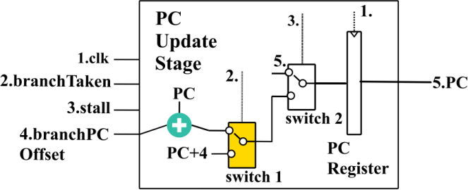
The first pipeline stage is the program counter register update (PCR) stage (see Figure 1 above). This stage updates the value of the program counter (PC) register. The input ports are the clk, branchTaken, stall and branchPCOffset. The positive edge of the clk is used to trigger an update to the PC pipeline register. The stall and branchTaken signals are used to select the next PC value. If the stall signal is active, the next PC value will be the same PC as the previous clock cycle. If the stall signal is inactive, but there is an active branchTaken signal, then the next PC value will be PC+branchPCOffset value. If neither of stall nor branchTaken signals are active, the next PC value will be set to PC + 4. Figure 1 represents the above implementation as two switches connected in series, switch 1 and switch 2. The part you need to modify in the code corresponds to switch 1 (shaded in yellow). See pcr.sv for the Verilog code.
Figure 2: Instruction Fetch (IF) Stage
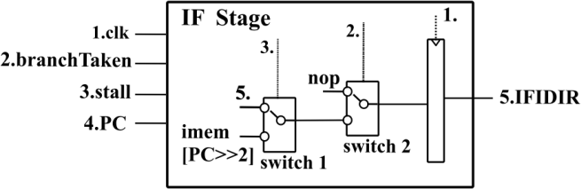
The Instruction Fetch (IF) stage (Figure 2) updates a new instruction into the IFIDIR register every positive clock edge. There are four inputs to the fetch stage. They are the clk, ijmpMem, stall and PC. There is one output of the fetch stage, the IFIDIR register value. The branchTaken signal indicates that a branch has changed the PC to a branched location. The stall signal indicates that there is a hazard between the decode stage and one of the other stages. Lastly, PC is the current PC value, from the PCR stage.
Every cycle, switch 2 checks the branchTaken signal. If true, it injects a nop into the IFIDIR register. Otherwise, switch 1 checks for a stall. If there is a stall, then it will updated IFIDIR with the same value as the previous cycle. Otherwise, it will update IFIDIR with a new instruction based on the word represented by PC at instruction memory location PC >> 2. See fetch.sv for the Verilog code corresponding to the Fetch stage. No modifications need to be made in this stage.
Figure 3: Instruction Decode (ID) Stage
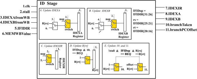
The Instruction Decode (ID) stage. It has six inputs and five outputs. The six inputs are clk, stall, IDEXAfromWB, IDEXBfromWB, IFIDIR and MEMWBValue.
clk and stall have the usual meanings as discussed above. IDEXAfromWB and IDEXBfromWB are signals indicating that there is an incoming writeback to either the rs or rt registers of the instruction being decoded. IFIDIR is the value of the pipeline register between the ID and IF stages. MEMWBValue contains the data from the WB stage that needs to be written into the register file.The outputs of the ID stage are IDEXIR, IDEXA, IDEXB, branchTaken and branchPCOffset.
There are five components in the decode section. Components A and B update the IDEXA and IDEXB pipeline registers, either with nop, or using the values of R[rs] or R[rt], or using the data forwarded from the WB stage. Component C updates the IDEXIR pipeline register either using nop or the IFIDIR value received from the IF stage. Component D needs to be added by you to update the contents of R[rt] using our definition of the BEQINIT instruction (see Problem 2). Component E needs to create the control signals branchTaken and branchPCOffset by evaluating whether the branch condition R[rs] == R[rt] is true. The changes in logic you need to make are are shaded in yellow. See decode.sv for the Verilog implementation.
Figure 4: Execute (EX) Stage
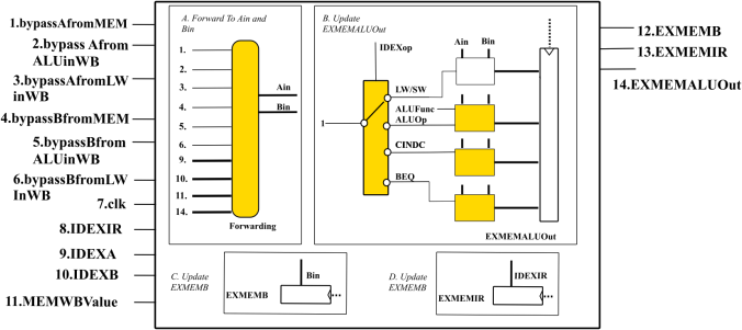
The Execute (EX) stage performs arithmetic operations. For example, an ALU type instruction like ADD, will carry out the addition in the execute stage.
The execute stage (see Figure 4) has eleven inputs to the execute stage, and four outputs. The eleven inputs include the six bypass signals, which are used in the forwarding circuit. They are
bypassAfromMem, bypassAfromALUinWB, bypassAfromLWinWB, bypassBfromMEM, bypassBfromALUinWB, bypassBfromLWinWB. The remaining input signals are the clk, IDEXIR, IDEXA, IDEXB and MEMWBValue. The output signals are from the pipeline registers EXMEMB, EXMEMIR and EXMEMALUOut.
There are four components. Component A is the forwarding unit which is used to create Ain and Bin, which are the values R[rs] and R[rt] corresponding to the instruction that needs to be executed. Component B carries out a computation on Ain and Bin. It stores the result in the EXMEMALUOut pipeline register. The ADD instruction is already implemented, but you’ll need to implement other ALUop, CINDC and BEQINIT instructions (see Problems 1,2 and 3). Component C propagates the Bin signal into the EXMEMB pipeline register, for use by the next pipeline stage MEM. Component D propagates the IDEXIR signal into the EXMEMIR pipeline register for use by the next pipeline stage MEM. You can implement the above logic (shaded in yellow) in execute.sv.
Figure 5: Forwarding Logic
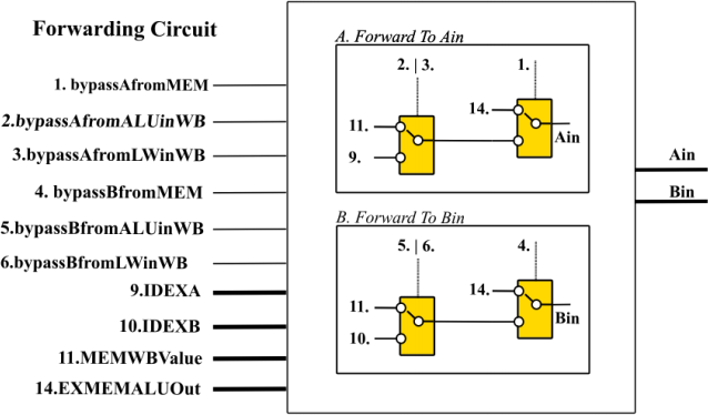
The forwarding circuit inside the ALU is presented in Figure 5. If any hazards are detected
relative to the MEM stage and the WB stage, then Ain and Bin will be modified to account for
those hazards. The forwarding logic has ten inputs and two outputs. The first group of signals are the ‘bypass’ control signals. They indicate whether forwarding needs to take place from
MEM to EX or WB to EX. bypassAfromMEM means that forwarding needs to take place from
MEM, on the first input to the ALUs, Ain. If bypassAfromALUinWB is true, forwarding needs to take place from the WB stage to Ain, due to an ALU type instruction in the WB stage. If
bypassAfromLWinWB is true, forwarding needs to happen due to an LW instruction in the WB stage. Similarly, there are three bypass signals for the Bin input. The IDEXA and IDEXB signals contain values of R[rs] and R[rt] obtained from the ID stage. They will be assigned to Ain and
Bin respectively, if none of the forwarding signals are true. EXMEMALUOut is the value that is forwarded from the MEM state. MEMWBValue is the value that is forwarded from the WB stage. You can implement the above logic (shaded in yellow) in forward.sv.
Other Phases:
The Memory (MEM) stage will access the memory for LW/SW instructions and do nothing for the others. The Writeback (WB) stage will access the register file and write to it.
There is also a control block, which generates the control signals which are input to these blocks. The code for the above stages need not be modified. All the modules are connected together in cpu.sv, which also does not need to be modified.
2.2 Test Cases :
In order to test the implementation, test cases have been provided in two folders, named specific_tests and random_tests. The specific tests target only a single instruction to be tested. The random tests contain random combinations of multiple instructions. Each test case consists of five .dat files, namely, dmem.dat, imem.dat, mem_result_expected.dat, regs.dat, and regs_result_expected.dat. The first three .dat files contain the initial state of the memory and registers. dmem.dat contains the initial data memory state, imem.dat contains the initial instruction memory state, and regs.dat contains the initial register state. The first line corresponds to r0, the second line to r1 and so on for the regs.dat file. Similarly, the first line corresponds to byte 0, the second line to byte 4 and so on, for the imem.dat and dmem.dat files. There are 32 registers in reg s.dat and 32 4-byte aligned memory locations in imem.dat and dmem.dat each.
The last two files mem_result_expected.dat and regs_result_expected.dat, should contain the final memory and register state once the execution has completed 2000 cycles and exited.
3. Executing the Test Cases Manually
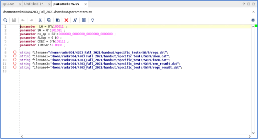
Create a new Verilog RTL project in Vivado. Import all the .sv files from the handout into your project. Change the paths in parameters.sv to the absolute path of the .dat files corresponding to the test case you want to simulate. The .dat files are found in the specific_tests and random_tests folders of the handout. Then execute the test case in Vivado using ‘Run Behavioral Simulation’ . The resultant memory registers state after simulation will be stored in two newly created files mem_result.dat and regs_result.dat, at the location you specified. Note that there are also two files mem_result_expected.dat and regs_result_expected.dat. You can compare the generated result files to the expected ones manually.
The absolute-path specification may be a little bit different depending on whether you are running Vivado on Windows or on Linux. On Windows, the absolute path needs to be specified using “\\” separators. For example, one possible command for reg s.dat on my windows laptop was
filename="C:\\Users\\Kartik\\Documents\\lab2\\reg s.dat";
On Linux, the “/” separator should be used. For example
filename="/home/ramkr004/lab2/reg s.dat";
3. 1 Observing Waveforms
A useful tool to debug your modifications to the processor, is to observe the waveform for different components of the processor.
i. Change the paths of the filenames, as mentioned above. One example path is shown in the screenshot below, which points to a test case that uses an ‘addition’ instruction, in the specific_tests folder.
ii. Run the simulation, using Vivado, using ‘ Run Behavioral Simulation’ .
Click on “ Run Simulation > Run Behavioral Simulation” . This should open the following window, as shown below.
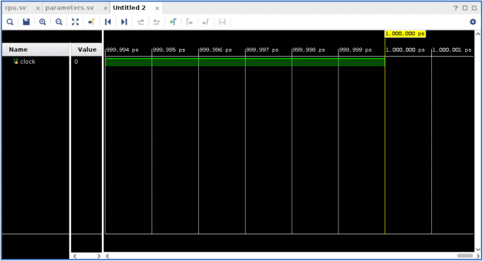
Click on ‘ Untitled 1’ , which should open a waveform window. Then click ‘cpu’ in the Scope window. The Vivado display should now look like the following :
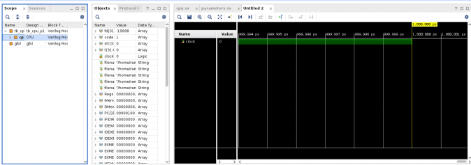
Drag and drop the clock signal, the pipeline intermediate register signals, IFIDIR, IDEXIR, EXMEMIR and MEMWBIR, and the program counter PC, into the ‘ Name’ column of the waveform window. Then, click on the ‘ Relaunch Simulation’ icon on the top toolbar to populate these waveform shapes. The waveform window should now look like below :
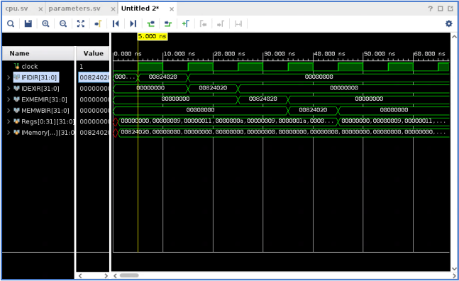
The four intermediate registers shown here are IFIDIR, IDEXIR, EXMEMIR, MEMWBIR. These intermediate pipeline registers store the instructions in binary form as they propagate through the pipeline. IFIDIR is between the IF (fetch) and ID (decode) stage, IDEXIR is between the ID and EX (execute) stages, EXMEMIR is between the EX and MEM (memory) stages, and MEMWBIR is between the MEM and WB (writeback) stages.
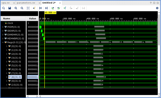
Changes to the register state can also be observed :
3. 2 Manually Using The Dat Files
The state of registers and the memory at the end of the simulation, can be manually inspected. The result of the execution can be used to check correctness.
regs.dat has the following initialization:
00000000000000000000000000000000
00000000000000000000000000001001
00000000000000000000000000010001
00000000000000000000000000001010
00000000000000000000000000001001
00000000000000000000000000011010
00000000000000000000000000010010
00000000000000000000000000000011
00000000000000000000000000011100
00000000000000000000000000010100
00000000000000000000000000011011
00000000000000000000000000000111
00000000000000000000000000010110
00000000000000000000000000001110
00000000000000000000000000010011
00000000000000000000000000001001
00000000000000000000000000000110
00000000000000000000000000001101
00000000000000000000000000010001
00000000000000000000000000000011
00000000000000000000000000000101
00000000000000000000000000000101
00000000000000000000000000011000
00000000000000000000000000011110
00000000000000000000000000001011
00000000000000000000000000001101
00000000000000000000000000011011
00000000000000000000000000010100
00000000000000000000000000001110
00000000000000000000000000010100
00000000000000000000000000000001
00000000000000000000000000011100
dmem.dat has the following values:
00000000000000000000000000000110
00000000000000000000000000010011
00000000000000000000000000011111
00000000000000000000000000001100
00000000000000000000000000001101
00000000000000000000000000001011
00000000000000000000000000011011
00000000000000000000000000000110
00000000000000000000000000000010
00000000000000000000000000011000
00000000000000000000000000001000
00000000000000000000000000001101
00000000000000000000000000011010
00000000000000000000000000000011
00000000000000000000000000011111
00000000000000000000000000011010
00000000000000000000000000010010
00000000000000000000000000010111
00000000000000000000000000011000
00000000000000000000000000011010
00000000000000000000000000011101
00000000000000000000000000010111
00000000000000000000000000001001
00000000000000000000000000010100
00000000000000000000000000010010
00000000000000000000000000000110
00000000000000000000000000010100
00000000000000000000000000010001
00000000000000000000000000000010
00000000000000000000000000000001
00000000000000000000000000011101
00000000000000000000000000000111
imem.dat has the following initialization:
00000000100000100100000000100000
00000000000000000000000000000000
00000000000000000000000000000000
00000000000000000000000000000000
00000000000000000000000000000000
00000000000000000000000000000000
00000000000000000000000000000000
00000000000000000000000000000000
00000000000000000000000000000000
00000000000000000000000000000000
00000000000000000000000000000000
00000000000000000000000000000000
00000000000000000000000000000000
00000000000000000000000000000000
00000000000000000000000000000000
00000000000000000000000000000000
00000000000000000000000000000000
00000000000000000000000000000000
00000000000000000000000000000000
00000000000000000000000000000000
00000000000000000000000000000000
00000000000000000000000000000000
00000000000000000000000000000000
00000000000000000000000000000000
00000000000000000000000000000000
00000000000000000000000000000000
00000000000000000000000000000000
00000000000000000000000000000000
00000000000000000000000000000000
00000000000000000000000000000000
The instruction in the first word is ‘add r8, r4, r2’ .
Let’s break this into the fields of an instruction word in MIPS to understand it.
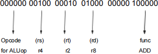
r2 is initialized to 10001 (in binary), as specified by reg s.dat. The value of r4 is 1001. Lastly the value in r8 is initialized to 111000. The generatedregs_result.dat should show that r8 has value r4 + r2, which is 11010. All other instructions in memory are initialized to 0, which represents nop instructions.
regs_result.dat shows the final output of the register file - result after executing the instructions from the test case.
00000000000000000000000000000000
00000000000000000000000000001001
00000000000000000000000000010001
00000000000000000000000000001010
00000000000000000000000000001001
00000000000000000000000000011010
00000000000000000000000000010010
00000000000000000000000000000011
00000000000000000000000000011010
00000000000000000000000000010100
00000000000000000000000000011011
00000000000000000000000000000111
00000000000000000000000000010110
00000000000000000000000000001110
00000000000000000000000000010011
00000000000000000000000000001001
00000000000000000000000000000110
00000000000000000000000000001101
00000000000000000000000000010001
00000000000000000000000000000011
00000000000000000000000000000101
00000000000000000000000000000101
00000000000000000000000000011000
00000000000000000000000000011110
00000000000000000000000000001011
00000000000000000000000000001101
00000000000000000000000000011011
00000000000000000000000000010100
00000000000000000000000000001110
00000000000000000000000000010100
00000000000000000000000000000001
00000000000000000000000000011100
The r8 register has been updated.
mem_result .dat has the following result.
00000000000000000000000000000000
00000000000000000000000000001001
00000000000000000000000000010001
00000000000000000000000000001010
00000000000000000000000000001001
00000000000000000000000000011010
00000000000000000000000000010010
00000000000000000000000000000011
00000000000000000000000000011010
00000000000000000000000000010100
00000000000000000000000000011011
00000000000000000000000000000111
00000000000000000000000000010110
00000000000000000000000000001110
00000000000000000000000000010011
00000000000000000000000000001001
00000000000000000000000000000110
00000000000000000000000000001101
00000000000000000000000000010001
00000000000000000000000000000011
00000000000000000000000000000101
00000000000000000000000000000101
00000000000000000000000000011000
00000000000000000000000000011110
00000000000000000000000000001011
00000000000000000000000000001101
00000000000000000000000000011011
00000000000000000000000000010100
00000000000000000000000000001110
00000000000000000000000000010100
00000000000000000000000000000001
00000000000000000000000000011100
There is no change to the contents of the memory locations.
3. 2 Auto-Decoding Utility
A binary called ‘decode’ is provided. It should be placed in the same folder as an imem.dat file and executed, using ‘ ./decode’. This will generate a decoded version of imem.dat named decoded_imem.dat. For example, the result of running decode for the above example yielded: “add r8, r4, r2” .
4. Automated Execution And Grading
We support automatic grading of the assignment on Vole. Each instruction is tested using different memory and register states. For the ALU type instructions, there are two test cases for each of the instructions ADD, NAND, XOR, SRL and SGT. Thus, there are ten test cases for each of these instructions, but only two test cases per instruction are run by the grader. Two points are assigned for each test case that is graded. The total points is twenty for all these test cases combined.
For the remaining instructions CINDC and BEQINIT, ten test cases are provided. These are each worth two points. Thus, a total of twenty points is assigned for each instruction. The remaining twenty points are based on test cases that are random sequences of instructions. Forty test cases have been provided, each of which is worth one point.
In order to run all these test cases, a script is provided to you. Use the command ./grade.sh. It will take one hour or more time to complete grading all the test cases. A file ‘score.txt’ is created, which contains your score for each of the test cases. Please do your automatic grading on Vole because the grader has not been tested in other environments.
5. Problems
5. 0 Problem 0 (20 points):
Currently, an ADD instruction has been implemented in the execute.sv file.
Modify execute.sv so that it can run XOR, NAND, SGT (Set Greater Than) and SRL (Shift Right Logical Variable) instructions.
Hint : You need to modify the EX stage so that the ALU performs these operations. The function codes for XOR, NAND, SGT, and SRL are 50, 51, 52 and 53, respectively.
ADD performs the operation R[rd] = R[rs]+r[rt] (already implemented)
XOR performs the operations R[rd] = (R[rs] ^ R[rt])
NAND performs the operations R[rd] = (~(R[rs] & R[rt]))
SGT performs the operation R[rd] = (R[rs] > R[rt])
SRL performs the operation R[rd] = (R[rs] >> R[rt])
Hint :
Fill in the TODO parts (marked in the comments) of the provided code.
5. 1 Problem 1 (20 points) :
Add support for the “conditional increment decrement” instruction (opcode 47), which uses the ‘ R’ instruction format and is defined as follows :
cindc $rs, $rt, $rd
if (R[rs] > 0) R[rd] = R[rs] - R[rt]
else R[rd] = R[rs] + R[rt]
We need to modify the ID stage.
Hint: Fill in the TODO parts (marked in the comments) of the code.
5. 2 Problem 2 (20 points) :
Augment the given MIPS design so that it can run the “branch if equals to absolute address” instruction (opcode 48) which uses the ‘ I’ instruction format and is defined as follows :
beqin it $rs, $rt, offset
if (R[rs]=R[rt]) {
PC = PC + offset
R[rt] = 1
}
Key modifications to the code are in the ID stage.
Hint: Fill in the TODO parts (marked in the comments) of the code in decode.sv.
5. 3 Problem 3 (40 points) :
In this part of the problem, we create sequences containing different kinds of instructions, to see whether they can work together. A key part of this problem is to implement data forwarding. There are two kinds of forwarding which need to be implemented, which need to assign the values for Ain and Bin in forward.sv. This part also checks whether your BEQINIT instruction works because incorrect branching may cause an incorrect result. It also checks your CINDC results because incorrect CINDC results can cause a wrong overall register and memory state.
The random tests in the folder random_tests are used to generate random instruction sequences where forwarding may occur. One point is assigned for each test case.
Hint :
Fill in the TODO parts (marked in the comments) of the code in forward.sv.
5. 4 Test Cases :
There are totally seventy test cases which will be evaluated by the autograder. Ten test cases are for the new ALU instructions. Another twenty test cases are for the CINDC and BEQ instructions, ten for each instruction. There are forty test cases which are arbitrary mixes of all of these instructions. They also include predefined instructions such as LW and SW. Use the automatic grading (see 4.) to run all these test cases and obtain a score. Two points are assigned per test case for the specific test cases and one point per test case for the random test cases.
5. 4 Handout :
You are provided with an incomplete MIPS-like behavioral model (i.e. only the components required for this lab assignment), two testcase folders specific_tests and random_tests, this pdf and an automatic grader to calculate your score.
5. 5 Handin :
You only need to submit your modified pcr.sv, execute.sv, fetch.sv, decode.sv, mem.sv, wb.sv and forward.sv files on Canvas.
5. 6 Grading Criteria :
Credit is assigned based on the provided test cases. It is also possible to assign partial credit based on your implementation if your solution does not work. Please write your code neatly and comment on it, this is to your advantage.
5. 7 Important :
Please verify that your code can be simulated by Vivado to completion. Code that does not complete simulation will not receive full credit.
2023-12-20