CSE/ELE 664 – Intro. To SoC Design, Fall 2023 Project part 2
Hello, dear friend, you can consult us at any time if you have any questions, add WeChat: daixieit
CSE/ELE 664 – Intro. To SoC Design, Fall 2023
Project part 2: 32-bit microprocessor
CONTENT
1. Modules and I/Os ........................................................................................................................................ 1
2. Test Bench Design ....................................................................................................................................... 4
3. What to Turn In ........................................................................................................................................... 4
In this part of the project, you will build a 32-bit microprocessor that supports the given instruction set. The following table summarizes the supported instructions and their OPCODE. More detailed information on the instruction set has been introduced in the lecture.
|
Name mnemonic F Function Opcode/Func |
||||
|
Add |
add |
R |
R[rd]=R[rs]+R[rt] |
0/20hex |
|
Add Imm |
addi |
I |
R[rt]=R[rs]+signExtImm |
8hex |
|
And |
and |
R |
R[rd]=R[rs]&R[rt] |
0/24hex |
|
And Imm |
andi |
I |
R[rt]=R[rs]&ZeroExtImm |
Chex |
|
B on EQ |
beq |
I |
If(R[rs]==R[rt])PC=PC+4+BranchAddr |
4hex |
|
B on NEQ |
bne |
I |
If(R[rs]!=R[rt])PC=PC+4+BranchAddr |
5hex |
|
Jump |
j |
J |
PC=JumpAddr |
2hex |
|
Jmp & Lnk |
jal |
J |
R[31] = PC, PC = JumpAddr |
3hex |
|
Jmp Reg |
jr |
R |
PC = R[rs] |
0/08hex |
|
Subtract |
sub |
R |
R[rd]=R[rs]-R[rt] |
0/22hex |
|
Nor |
nor |
R |
R[rd]=~(R[rs]|R[rt]) |
0/27hex |
|
LD Word |
lw |
I |
R[rt]=M[R[rs]+SignExtImm] |
30hex |
|
ST Word |
sw |
I |
M[R[rs]+SignExtImm]=R[rt] |
2bhex |
|
Shift left |
sll |
R |
R[rd]=R[rt] << shamt |
0/00hex |
|
Shift right |
srl |
R |
R[rd]=R[rt] >> shamt |
0/02hex |
|
No op |
nop |
I |
No operation |
3Fhex |
|
Stall |
stll |
I |
PC = PC |
06hex |
1. Modules and I/Os
The top-level block diagram of the 32-bit microprocessor is given in the following figure. They are partitioned into several modules. The ALU module should be taken from your part 1. In this project, you need to complete the design of the controller, program counter, the top level, and the test bench. The green bounding-box modules are provided for you. You also need to verify the behavior of the microprocessor at RT level.
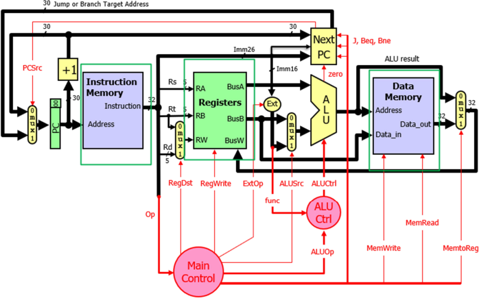
Figure 1: Reference Block Diagram of the 32-bit Microprocessor Architecture
The outputs from the controller are mainly the select and control signals to the datapath (select lines of multiplexers, de-multiplexers, address decoder for register bank, control signals for program counter, ALU, data memory and so on). The output of the program counter is the instruction memory address.
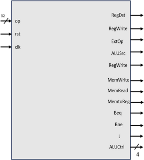
Figure 2: Block Diagram of Controller (Input/Output)
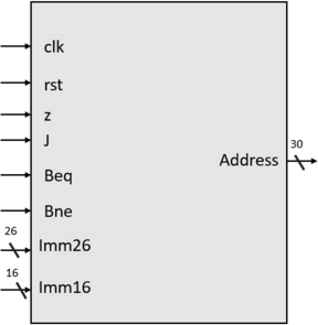
Figure 3: Block Diagram of Program counter (Input/Output)
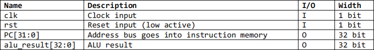
The input/output of the 32-bit microprocessor is specified in the following Table:
2. Test Bench Design
Your test bench should consist of one memory bank. The other expected of memory stores the cycle accuracy expected value of the ALU(i.e. PC and alu_result). The test bench should be able to report an error when there is a mismatch between the actual and expected output.
Your test program should cover different execution scenarios and all instructions in the instruction set. The following test cases includes parts of instructions, you should implement the TODO parts and all other instructions.
|
0.RESET = 1 |
|
|
|
Assembly Code: |
Test_bench code: |
Explanation: |
|
1: addi r1 r0 0x1 |
20010007 |
//pc =0, r1<- r0+0x7, r1=7; |
|
2. addi r2 r0 0x3 |
20020003 |
//pc =1, r2 <-r0 +r1, r2 =1; |
|
2. and r4 r1 r2 |
00222024 |
// pc =2 r4 <-r1&r2, r4 = 3; |
|
3. beq r0 r1 0x3 |
10000003 |
//pc =3 jump to pc =3+1+imm if r0 ==r1; |
|
4. stll |
18000000 |
// pc =4 STALL |
|
5. stll |
18010001 |
//pc =5 STALL |
|
6. stll |
18000002 |
// pc =6 STALL |
|
7. lw r0 r8 0x9 |
C0080009 |
// pc=7, load r [8] <-M [r [0] +9] |
8. to …. Add other instructions, and the last instruction should be Jump Reg to your STLL instruction.
3. What to Turn In
Complete the Verilog design for the controller, the ACC, the top level system, and the test bench of the system.
Create a test vector to check the function your processor. The data path of this simple processor is not pipelined. Each instruction takes two clock cycles. Please hand in the following items:
1. The zipped file of your working directory (including all Verilog source code, and the test vectors) 2. A report, which includes
a. The FSM diagram of your controller
b. The assembly code of your test program
c. The simulation waveform, in which the important steps (that indicate the correct function of the microprocessor) are labeled and explained.
I will first run your design using your own test bench, then copy your program_counter.v, ALU.v, controller.v and processor.v to my working directory and test it using my testbench and test vector. It is extremely important that you follow the given I/O specifications, make sure that the name of the top level module is called “ processor”, and do not change the provided Verilog code, otherwise, your design will not work in my environment.
2023-12-18
32-bit microprocessor