ELEC211 DIGITAL ELECTRONICS AND MICROPROCESSOR SYSTEMS SECOND SEMESTER EXAMINATIONS 2022/23
Hello, dear friend, you can consult us at any time if you have any questions, add WeChat: daixieit
ELEC211
SECOND SEMESTER EXAMINATIONS 2022/23
DIGITAL ELECTRONICS AND MICROPROCESSOR SYSTEMS
Section A
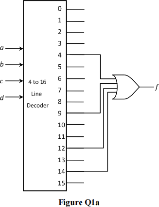
![]() 1. a) Find the minimum sum of products expression for the function f, given by the
1. a) Find the minimum sum of products expression for the function f, given by the
circuit shown in Figure Q1a, which uses a 4-to- 16 line decoder and an OR gate. (The most significant bit is a and the least significant bit is d.) Show working- out for your simplification.
![]() b) Design a circuit to implement the same function f from Question 1(a), using an 8-to- 1 multiplexer. Use a, band c as the select inputs, and das a data input.
b) Design a circuit to implement the same function f from Question 1(a), using an 8-to- 1 multiplexer. Use a, band c as the select inputs, and das a data input.
You can still assume that a is themsband d is the lsb.
Hint: you may find it easiest to start with the un-simplified form off (sum of minterms).
c) The Quine-McCluskey method is used to minimise the following Boolean
expression: f(a, b, C, d, e) = ∑ m(9, 16, 18,23) + ∑ d(1, 17, 19) where m represents the minterms for which f must be true and the terms following dare “don’tcare”. The lsb is e.
Column II of the method is given to you correctly below in Figure Q1c. Use this, with suitable working out or explanations, to write down:
i) Column III
ii) the Prime Implicant(s) of f
iii) the Essential Prime Implicant(s).
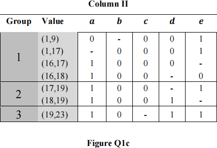
(Note: you are not required to determine the final minimum sum of products, or to write out Column II again with annotations.)
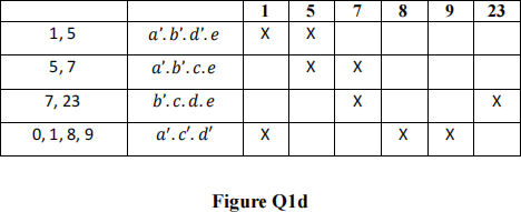
d) A Prime Implicant chart is shown correctly for a different function, g, in
Figure Q1d. Based on this chart, it is claimed that the minimum sum of products expression is g = b’ . C. d. e + a′ . C′ . d′ . Is this correct? If so, explain why. If not, explain why not, and suggest a correct expression.
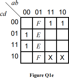
e) Find the minimum sum of products expression for the function G given by the following Karnaugh map (Figure Q1e) with map entered variables E and F.
Total 25
2. a) A state transition table for a finite state machine is shown in Figure Q2a, along with a key to the state names.
i) Is this a Moore or a Mealy machine? Explain how you could tell from the state transition table.
ii) Does the table use ‘One-Hot’ or ‘Encoded’ state representation? Explain how you could tell from the table or key.
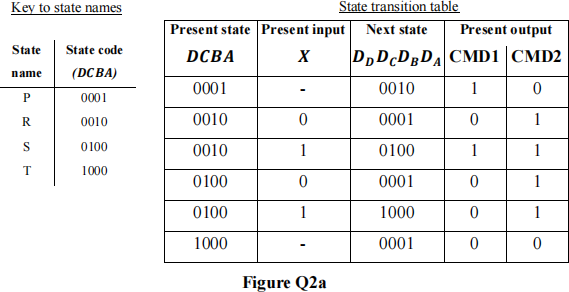
![]() b) Construct an ASM chart for the finite state machine described in Figure Q2a. Include the code for each state above the top-right of the state box, and its name above the top-left.
b) Construct an ASM chart for the finite state machine described in Figure Q2a. Include the code for each state above the top-right of the state box, and its name above the top-left.
![]() c) For the state machine described in Figure Q2a, design two simplified Boolean
c) For the state machine described in Figure Q2a, design two simplified Boolean
equations for the output CMD2, and the next state of flipflop A, assuming DFFs are used. A circuit diagram is not required. You can work from the state transition table or directly from your ASM chart.
As examples to help, you are given:
CMD1 = A + B. X
DB = A
DC = B. X
DD = C. X
d) A 4-bit adder is to be designed for a microprocessor. The clock frequency is 50 MHz, and the logic gates used each have a propagation delay of 3 ns and a fan-in of 5.
i) Explain why a serial adder cannot perform 4-bit addition in one clock cycle.
A 4-bit Carry Look-Ahead (CLA) adder design is proposed (Figure Q2d):
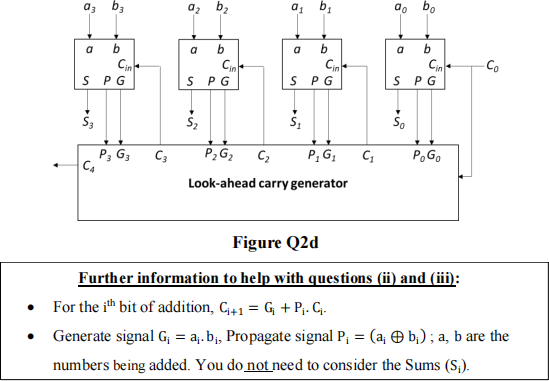
ii) Sketch a simple Generate/Propagate logic circuit for finding C1 from inputs a0 , b0 and C0 . Then, by writing down equations for C1−4 involving G and P, and doing some calculations, demonstrate that it will take the CLA less than one clock cycle to determine the carry-out from the fourth bit (c4).
iii) It is proposed to allow 8 bits of addition by simply extending the circuit in Figure Q2d to the left, with 4 more bits of addition and look-ahead carry logic. Briefly explain why the fan-in of the gates would cause a problem with this.
Total 25
Section B
|
3. |
a) |
Explain what each of the following parts of the CPU does: i) instruction register, ii) instruction decoder, and iii) address register. |
|
|
b) |
Assume that the following registers initially hold the values given: r5: 0x0001048D r6: 0x3C2A0919 r7: 0xE0F27D62 r15: 0x00001010 Find the values held in registers r3, r4, r5, r7 and r15 (PC) after the following ARM Cortex M0 instructions are executed sequentially. i) MOV r4, r5 ii) ORR r5, r6 iii) ADDS r3, r6, r7 iv) RORS r7, r7, r4 |
|
|
c) |
Find the 32 bit two's complement format for the decimal numbers: i) -5710 ii) -575,757,57510. (Note that 0x22515D07 is the hexadecimal |
equivalent of +575,757,57510.)
numbers:
i) -5.7510
ii) +75.410.
Total 25
4. a) What advantages does the two’s complement method have compared to the sign magnitude method?
b) Find the decimal number represented by 0xFFFFF5E6 using the 32 bit two’s complement format.
c) The ARM Cortex M0 microprocessor has four flags, namely N (negative), Z (zero), C (carry) and V (overflow).
Find the value held in register r5 and determine the state of the flags after the execution of the instruction:
ADDS r5, r5, #0x9E ; add 15810 tor5 and put sum in r5
i) when the value held by r5 is 0xFFFFFF62
ii) when the value held by r5 is 0x7FFFFF6F
iii) when the value held by r5 is 0xFFFFFF61
d) This question assumes that the value held in register r7 is 0x00400000 and that the following memory locations hold the following values:
Memory address Contents
0x00400000 0x01
0x00400001 0x02
0x00400002 0x03
0x00400003 0x04
0x00400004 0x05
0x00400005 0x06
Assuming that the computer memory is little endian, determine the contents of registers r0, r1 and r2 after the following ‘load register’ instructions are
executed sequentially.
i) LDRB r2, [r7, #1] ; load byte
ii) LDRSH r1, [r7, r2] ; load signed half word
iii) LDR r0, [r7] ; load word
Total 25
2023-08-24