ELEC211 DIGITAL ELECTRONICS AND MICROPROCESSOR SYSTEMS SEMESTER TWO EXAMINATION 2020/21
Hello, dear friend, you can consult us at any time if you have any questions, add WeChat: daixieit
ELEC211
SEMESTER TWO EXAMINATION 2020/21
DIGITAL ELECTRONICS AND MICROPROCESSOR SYSTEMS
Section A
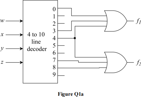
![]() 1. a) Find sum of products expressions for the functions f1 and f2 given by the circuit
1. a) Find sum of products expressions for the functions f1 and f2 given by the circuit
shown in Figure Q1a using a BCD to decimal decoder, where w is themsb and z
is the lsb. (You are not required to simplify the resultant expressions.)
b) Design a circuit to implement the following function using an 8-to- 1 multiplexer:
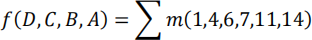
c) The Quine-McCluskey method is used to minimise the following Boolean expression:

Where m represents theminterms for which f must be true, and the terms following dare “don’t care”. Themsb is A.
Note: you are not required to perform the whole minimisation procedure; you only need to answer the following questions.
i) Identify and explain three mistakes in the Prime Implicant chart for the above problem, shown in Figure Q1ci. (Note: the first column of the chart is correct.)
ii) Write down your corrected Prime Implicant chart. Use it to find the Essential Prime Implicant(s), and the final minimum sum of products expression. Explain any decision(s) you have to make for the minimum sum of products.
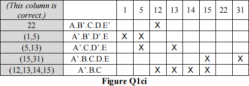
d) Find the minimum sum of products expression for the function G given by the following Karnaugh map with map entered variables E and F.
Total 25
2. a) An ASM chart for a finite state machine is shown in Figure Q2a.
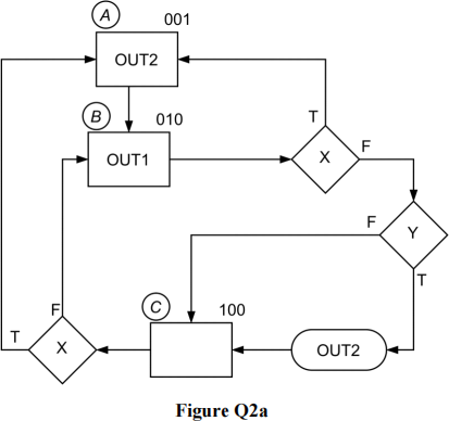
i) Design a PLA table to implement the logic of the present outputs and next states, for the ASM chart shown in Figure Q2a. Use the letters P, R and S as flipflop state variables, so that e.g. SRP = 001 represents state A. Table headings are given below to help you begin:
ii) For the ASM chart shown in Figure Q2a, design simplified Boolean equations for the present outputs and next-state logic, assuming DFFs are used. A circuit diagram is not required.
b) You are asked to design a 16-bit adder circuit for a microprocessor, with the following design constraints (note that compound gates are not used):
• The result (that is, the final sum) should be stable within one clock cycle
• The clock frequency is 40 MHz
• The logic gates used each have a propagation delay of 2 ns
• The design is based around the 1-bit adder circuit shown in Figure Q2b.
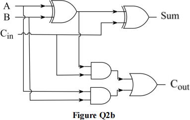
![]() i) Explain, including calculations, why neither a serial adder, nor a parallel ‘ripple carry’ adder, could satisfy the constraints above.
i) Explain, including calculations, why neither a serial adder, nor a parallel ‘ripple carry’ adder, could satisfy the constraints above.
ii) Explain how a ‘carry look-ahead adder’ (CLA) design using four 4-bit CLA blocks could satisfy the specific constraints above. Include relevant equations and calculations; you may also include a circuit diagram(s) to support your explanation.
Hints: Start by calculating the maximum delay from C0 to Sum (where C0 is the carry-into the whole circuit) across a 4-bit adder block using propagate/generate and carry look- ahead logic. This should come to 8 ns (you will need to explain why). Secondly, extend your design to 16-bit addition using group propagate/generate and a further layer of CLA logic.
Assume that all gates, including XOR, have a delay of 2 ns.
Total 25
Section B
|
3. |
a) |
Given the following Assembly language program for the ARM Cortex M0 using a little endian configuration: AREA asm_prog, CODE, READONLY THUMB EXPORT start start PROC ; Start of the program 0x00004004 LDR r0, =0x00010000 0x00004006 LDR r1, =0x5CB6B32F 0x00004008 LDR r2, =0x3D2D7B4B 0x0000400A LDR r3, =0xF100F100 0x0000400C LDR r4, =0x88011022 i) 0x00004014 ADDS r1, r1, r2 ii) 0x00004016 BICS r2, r3 iii) 0x00004018 ASRS r3, r0, #0x04 iv) 0x0000401A STRH r4, [r0] ENDP END ; End of the program Assuming that register r15 initially holds the value 0x00004004, find the values held in registers r1, r2, r3 and in the memory after the instructions (i) to (iv) are executed. For each executed instruction you are required to provide: • the procedure to calculate the result value after the instruction is executed. • the status of the modified register(s) after the execution of the instruction. • the status of the memory, only if it changes. |
|
b) The 32-bit two's complement number 0xFFFFF81B is stored in one of the ARM Cortex M0 registers. What is its decimal representation?
c) Find the IEEE 754 floating point format (single precision) for the decimal numbers:
i) -415.510
ii) +41.310.
d) Find the decimal number that is equivalent to 0xC4610000 in the IEEE 754 floating point format.
i) - 1910
ii) - 1,919,191,91910. (Note that 0x72648B6F is the hexadecimal
equivalent of +1,919,191,91910.)
Total 25
4. a) You have been asked to design an Assembly language program for the ARM
Cortex M0 to add the two positive integers greater than 4.3 根109.
i) Write the Assembly language program to perform 5根1010 + 5根1011
(0xB A43B7400 + 0x74 6A528800).
ii) Show step by step working of the program you wrote in Q4.a)i) above, including contents of each relevant register, and how the final value is
obtained.
b) The ARM Cortex M0 microprocessor has four flags, namely N (negative),
Z (zero), C (carry) and V (overflow).
Find the value held in register r4 and determine the state of the flags after the
execution of the instruction:
ADDS r4, r1, #0xE3 ; add 22710 tor1, put sum in r4
i) when the value held by r1 is 0xFFFFFF1D
ii) when the value held by r1 is 0x00C18000
iii) when the value held by r1 is 0xFFFFFF00
c) Considering a microprocessor with a cache memory:
i) Draw a graph of the mean memory access time (tave) against the hit ratio
(h), which is within the range 0 and 1, when:
• Main memory access time tm = 50 ns;
• Cache access time tc = 25 ns;
• Extra time delay due to cache control and routing circuits a = 30 ns.
ii) What is the mean memory access time when h = 0.95?
Total
25
2023-08-24