ELEC271 Experiment 5 - Design of an Operational Amplifier Using Multisim
Hello, dear friend, you can consult us at any time if you have any questions, add WeChat: daixieit
ELEC271
Experiment 5 - Design of an Operational
Amplifier Using Multisim
Department of Electrical Engineering & Electronics
January 2021, Ver. 5.1
Instructions:
• The Pre-Lab Questions must be answered before the lab day (deadline is 9 am). They are available on Canvas ELEC273/224/222 Modules and worth 20%.
• This is a design experiment. You are expected to do work and self-study before the lab day. Read this script before attempting the experiment. Prepare the design before attending the lab to save time.
• Review Multisim software before attempting the experiment. Check Canvas for Multisim resources. See online material and resources as well.
• Keep a record of all schematics and results.
• Refer to the hints and guidance given in the lectures of Module ELEC271 whenever needed during the lab.
• Use the report template (available on Canvas) to write your formal report after the lab.
• If you have any feedback on your laboratory experience for today, please write it down in the last page of this script.
1. Learning outcomes
At the end of this lab, you will:
• be able to produce a functioning operational amplifier circuit by combining different stages.
• be aware of problems and challenges to meet a specification for designing and characterising an operational amplifier.
2. Objectives
It is required to design an operational amplifier with the aid of Multisim software to satisfy the following design specifications:
a) Differential input impedance greater than 100 kΩ .
b) Voltage gain (that is, ‘open loop gain’) greater than 500,000.
c) Output impedance less than 1 kΩ .
d) Output voltage to be approximately zero volts for zero input.
e) Frequency response down to dc (0 Hz).
f) Supply voltage ![]() 9 V.
9 V.
g) Total current consumption not greater than 5 mA.
3. Introduction
This experiment requires you to design and simulate an operational amplifier circuit. A practical integrated circuit version (e.g. a 741 type) would in addition contain a ‘push pull’ output stage and extra components to provide further temperature and supply variation immunity.
The experiment is intended to reinforce lecture material in module ELEC271, and reference to the relevant lecture notes is essential. Refer also to the preparatory slides/stream in the introductory lectures to Experiment 5.
3.1. Operational amplifier
An operational amplifier (op-amp) is a high-gain voltage amplifier with a differential input and a single-ended output [Figure 1 (a)]. It is among the most widely used electronic devices today, being used in a vast array of consumer, industrial, and scientific devices, with very low cost. The op-amps had their origins in analogue computers where they were used in many linear, non-linear and frequency-dependent circuits. Their popularity in circuit design largely stems from the fact that characteristics of the op-amp circuits with negative feedback (such as their gain) are set by external components with little dependence on temperature changes and manufacturing variations in the op-amp itself. Examples of op-amp circuits are shown in Figure 1 (b) and (c).
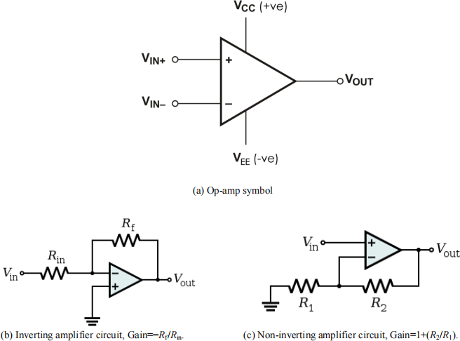
Figure 1. Operational amplifier and circuit applications
The op-amp is one type of a differential amplifier. Other types of differential amplifiers include the fully differential amplifier (similar to the op-amp, but with two outputs), the instrumentation amplifier (usually built from three op-amps), the isolation amplifier (similar to the instrumentation amplifier, but with added tolerance to common-mode voltages that would destroy an ordinary op-amp), and negative feedback amplifier (usually built from one or more op-amps and a resistive feedback network).
3.2. The design
The op-amp you are required to design can be constructed from four basic ‘building block’ circuits:
a) An emitter follower
b) A common emitter amplifier
c) A current mirror circuit
d) A differential input stage (long-tailed pair)
The designed operational amplifier schematic will be simulated using Multisim software library models located in the Components library. To place a component, open the ‘Select a Component’ window from the Place/Component menu (Ctrl+W) or by clicking on a component icon. In this experiment, two transistor types, npn and pnp, are used. You can find these transistors in the ‘Select a Component’ window:
• Q2N2222 npn transistor, from Transistors/BJT_NPN/PN2222.
• Q2N2907 pnp transistor, from Transistors/BJT_PNP/PN2907.
In the above notation, ‘Transistors’ is the Group, BJT_NPN (BJT_PNP) is the Family, and PN2222 (PN2907) is the Component name. This notation is used throughout this document. For example, to place a 2N2222 transistor, select ‘Transistors’ from Group, BJT_NPN from Family, and select PN2222 from the Component list. Alternatively, you can search for PN2222 in the search box below ‘Component’ .
The output from your differential amplifier should be fed into the input of the common emitter stage. It is also necessary to include an emitter follower circuit as a buffer between the two amplifier stages. Figure 2 shows a block diagram of the op-amp.
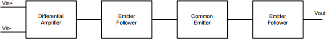
Figure 2. Block diagram of the op-amp
The properties of these blocks should have been investigated and design procedures established in the exercise ‘Pre-lab Test for Experiment 5’ . It is essential that this is done before commencing.
4. Experimental work
4.1. Part I: Transistor output characteristics
Objective: To obtain a set of output characteristics for the two transistor types to be used in this experiment.
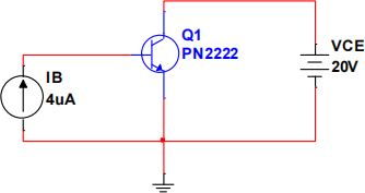
Obtain a plot of the output characteristics of the 2N2222 transistor, i.e. IC vs. VCE (0 to 20 V in steps of 0.1 V) for a range of IB (0 to 40 μA in steps of 4 μA).
Procedure:
• Task-1: Input the circuit schematic of Figure 3 in Multisim schematic worksheet. You can find the other components in ‘Select a Component’ window:
o Voltage source: Sources/POWER_SOURCES/DC_POWER.
o Current source: Sources/SIGNAL_CURRENT_SOURCES/DC_CURRENT.
o Ground: Sources/POWER_SOURCES/GROUND.
Double click on voltage source and current source and change their labels to VCE and IB, respectively.
• Task-2: To setup the simulation, click on the simulation setup icon (or from Simulation menu select Analysis and simulation). In the Analysis and Simulation window, select DC Sweep from the left panel. On the Analysis Parameters tab select VCE as the Source for Source 1 and IB as the Source for Source 2. Set the sweep parameters into the desired range, as indicated above. On the Output tab, select I(Q1[IC]) and add it to the Selected Variables for Analysis panel on the right.
• Task-3: Click on the run icon (green triangle) to start simulation. A response graph will appear. Take a screenshot of the graph. Alternatively, you can copy the graph and paste in a Word document.
• Task-4: From the graph, estimate the dc current gain, F (also known as hFE) at IC around
2 mA. Estimate also the ac (small signal) current gain, F0 (also known as hfe). Hint: see your notes on how to do this. Record your results.
![]()
Figure 3. Schematic diagram of Part I.
4.2. Part II: Achieving the specification of the operational amplifier [35 Marks]
Objective: To build the complete operational amplifier circuit and obtain the required specification.
Start now building the complete circuit of the operational amplifier (see the given ‘tutorial’ lecture for ELEC271 on Canvas).
Procedure:
• Task-1 [5 Marks]: Combine the required stages to build a complete operational amplifier in Multisim.
Hint: Match the differential amplifier and common emitter stages with an emitter follower stage, make the Rin(EF) ~ 10Ro(D)ut(A) .
• Task-2 [5 Marks]: Connect a signal source to one input and connect the other input to ground. Obtain the transfer characteristics of your amplifier by performing a DC Sweep from –9 V to +9 V. Identify the useful input voltage range from your plot. You will need to narrow the sweep range to achieve an accurate useful range.
• Task-3 [5 Marks]: Find the open loop gain (Aol) of the amplifier from the useful range in the above step.
• Task-4 [5 Marks]: Determine the required dc voltage offset from the transfer characteristic. Use this value to help balance the amplifier - you can apply a small dc offset to one of the inputs to try to centre the output close to zero volts. Hint: Alternatively, you could use the technique mentioned in the lecture notes to obtain Aol which would also give you the dc offset.
• Task-5 [5 Marks]: Obtain a set of input/output waveforms (in useful range) from a Transient simulation, and from which, calculate the gain of the amplifier. Verify that the specification has been met. Record your results.
• Task-6 [5 Marks]: Perform a Transfer Function simulation. Check the value of the gain and compare it to the value from your calculations and the value you found in Task-5. Check the values of the input and output impedance and compare them to your calculated values.
• Task-7 [5 Marks]: Place a few voltage, current, and power probes on different points of your schematic diagram (power probes should be placed on a component). Run an Interactive simulation and observe the voltage, current, or power showing by the probes.
Hint: You can double click on each probe and on the Parameters tab select the parameters that you want to be shown by the probe.
4.3. Part III: Obtaining the frequency response of the designed amplifier [10 Marks] Objective: To obtain the gain and phase Bode plots of the designed amplifier.
Now, obtain the frequency response of the designed amplifier by determining the gain and phase Bode plots.
Procedure:
• Task-1 [5 Marks]: You can find the frequency response of the amplifier by performing an AC Sweep simulation. In AC Sweep page in Analysis and Simulation window, on the Output tab, add the output voltage from the left panel to the Selected variables for analysis on the right panel (placing a voltage probe at the output makes it easier to find the output node in the list of variables). To draw the frequency response as Bode plots, on the Frequency parameters tab, select Sweep type: Decade and Vertical Scale: Decibel.
You can also obtain the frequency response of the other parameters, like the input impedance. In the AC Sweep page, on the Output tab, click on Add expression button. In the Expression field, write an expression for the input impedance in form of V/I. For example, if you have named your input signal source as V1, the expression for input impedance would be V(1)/I(V(1)).
• Task-2 [5 Marks]: Add a phase compensating capacitor (say 30 pF or any suitable value) between the collector of the common emitter stage and the base of the first emitter follower. Investigate the effect on the Bode plots. Copy the graphs and record your findings.
4.4. Bonus Part: Response to common-mode signal
Investigate the response of your amplifier to common-mode signals.
5. General questions
a) What can you deduce about the stability of your amplifier from the Bode plots in Part III?
b) What is the purpose of the ‘Phase compensating capacitor’?
6. Report writing guidelines for Experiment 5
• This experiment is assessed by means of a formal report. Use the formal report template (available on Canvas) to write your report. The idea behind this report is to document your experience and technical findings in this experiment.
• In your ‘Results’ section, include the following:
- All your findings and measurements along with a copy of all schematic diagrams and all simulation results. Make sure to comment on each result and simulation.
- The table shown overleaf (Table I) with your own results. Make sure to write relevant comments in the fourth column.
• In your ‘Discussions and Conclusions’ section include the following:
- Describe any problems you have experienced while carrying out both experiments and explain your problem-solving methods that you have followed.
- Include the answers to the general questions (Section 5 above).
- Does your designed op-amp achieve the specification? If not, explain the reasons.
• Important: Make sure that all of your figures (schematic diagrams and simulation results) are clear and all the numbers on the figures are readable.
Table I. Design specifications table
|
Parameter |
Specification |
Your value |
Comment on the value obtained |
|
Differential input impedance |
> 100 k |
|
|
|
Open loop voltage gain |
> 500,000 |
|
|
|
Output impedance |
< 1 k |
|
|
|
DC output voltage |
~0 V |
|
|
|
DC offset voltage |
None given |
|
|
|
Frequency response |
Down to DC (0 Hz) |
|
|
|
Total current consumption |
< 5 mA |
|
|
|
Bandwidth with compensation capacitor |
None given |
|
|
7. Report marking scheme
The report has 20 marks of the module. It will be marked out of 100% and then the mark will be scaled to 20%. The pre-lab test has 5 marks of the module.
The report marking scheme is as follows:
• Results of Part II (calculations, schematics, screenshots, etc.) with explanation and comments: 35 Marks
• Results of Part III (calculations, schematics, screenshots, etc.) with explanation and comments: 10 Marks
• The design specifications table with comments: 24 Marks
• Discussions and Conclusions section (including answers to the general questions of Section 5): 26 Marks
• Overall report presentation: 5 Marks
Note: High marks require very good comments and explanations.
8. Plagiarism and Collusion
Plagiarism and collusion or fabrication of data is always treated seriously, and action appropriate to the circumstances is always taken. The procedure followed by the University in all cases where plagiarism, collusion or fabrication is suspected is detailed in the University’s Policy for Dealing with Plagiarism, Collusion and Fabrication of Data, Code of Practice on Assessment, Category C, available on:
https://www.liverpool.ac.uk/media/livacuk/tqsd/code-of-practice-on-
assessment/appendix_L_cop_assess.pdf
Follow the following guidelines to avoid any problems:
a) Do your work yourself.
b) Acknowledge all your sources.
c) Present your results as they are.
d) Restrict access to your work.
References
[1] S Hall, Lecture notes-Module ELEC271, 2015.
Version history:
|
Name |
Date |
Version |
|
N Sedghi |
January 20201 |
Ver. 5.1 |
|
N Sedghi |
July 2020 |
Ver. 5.0 |
|
M López-Benítez |
September 2019 |
Ver. 4.1 |
|
A Al-Ataby |
February 2015 |
Ver. 4.0 |
|
A Al-Ataby |
February 2014 |
Ver. 3.2 |
|
A Al-Ataby |
February 2013 |
Ver. 3.1 |
|
A Al-Ataby |
March 2012 |
Ver. 3.0 |
|
S Hall |
September 2011 |
Ver. 2.2 |
|
S Hall |
March 2011 |
Ver. 2.1 |
|
T Dowrick/S Hall |
December 2009 |
Ver. 2.0 |
|
T Dowrick/S Hall |
August 2008 |
Ver. 1.0 |
2023-03-17