ELEC0010 Digital Design lab
Hello, dear friend, you can consult us at any time if you have any questions, add WeChat: daixieit
ELEC0010 Digital Design lab
Design and test activities:
1. Arithmetic Logic Unit (ALU)
2. Register file
3. Combined ALU and register file
4. Read-only memory (ROM)
5. Program counter
6. Combining the ROM with program counter
7. Control unit
8. Complete CPU design
Introduction
In these lab activities, you will design and simulate the central processing unit (CPU) microarchitecture shown below. Read the accompanying notes on microprocessor architecture and implementation, before starting the design activities.
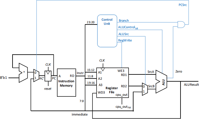
The components you will implement are: the arithmetic logic unit (ALU), the register file, the program memory, the program counter and the control unit. You will then combine these in a hierarchical design to implement the microprocessor, and program it with simple machine code instructions. To assist you with your designs, you can refer to the document ‘Example SystemVerilog modules’ on Moodle.
The SystemVerilog code should be written in Visual Studio Code editor, simulated using Icarus Verilog and the simulation waveforms plotted using GTKWave. Refer to the guide to using these tools on Moodle.
Write a lab report, presenting the SystemVerilog code for each module , the associated testbench code, and the simulation results (input and output signal values and waveforms). The marks awarded for each activity are specified at the bottom of each page.
1. Arithmetic logic unit (ALU)
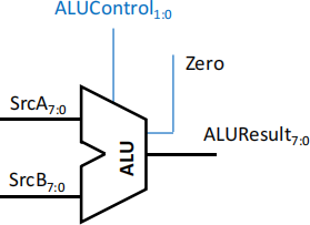
|
Module name |
alu |
|
Output ports |
ALUResult[7:0], Zero |
|
Input ports |
SrcA[7:0], SrcB[7:0], ALUControl[1:0] |
Write, as a SystemVerilog module with the name alu, a behavioural description of an arithmetic logic unit.
The data inputs, SrcA and SrcB, and the data output, ALUResult, are 8-bit vectors. The ALUControl input is a 2-bit vector.
The 1-bit output flag Zero = 1 if ALUResult == 0, else Zero = 0. The ALU carries out bitwise logical operations, and addition and subtraction operations, as specified in the table below.
|
ALUControl |
Operation |
Description |
|
00 |
a & b |
Bitwise logical operation: a AND b |
|
01 |
a | b |
Bitwise logical operation: a OR b |
|
10 |
a + b |
Arithmetic operation, addition: a + b |
|
11 |
a − b |
Arithmetic operation, subtraction: a − b |
Note that, in SystemVerilog, negative values are represented in 2’s-complement, so for example, 410 − 710 = −310 would be implemented as:
000001002 + 111110012 = 111111012 , or, expressed in hexadecimal: 0x04 + 0xF9 = 0xFD
Write a testbench to test the ALU. Since it’s infeasible to test your design with all possible input vectors (there are too many), it is sufficient to test each of the ALU operations using one set of test vectors (input values). Carry out the simulation using Icarus Verilog. [10 marks]
2. Register file
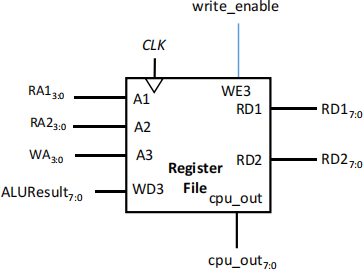
|
Module name |
reg_file |
|
Output ports |
RD1[7:0, RD2[7:0], cpu_out[7:0] |
|
Input ports |
RA1[3:0], RA2[3:0], WA[3:0], ALUResult[7:0], write_enable, CLK |
The register file has sixteen 8-bit registers. The register with address 0 always contains the value 0. The other 15 registers can have values written into them through the WD3 port.
The contents of any two of the registers (with addresses specified by the 4-bit inputs RA1 and RA2) are continuously output as RD1 and RD2. On the positive edge of the clock, if write_enable is asserted, and A3 > 0, the input ALUResult is written into the register at address A3 through the WD3 port.
The module includes an output port cpu_out7:0 , which continuously outputs the contents of the register at address 15. This will form the main external output of the microprocessor.
Write a SystemVerilog module, with the name reg_file, implementing this register file.
Write a testbench to simulate your register. Test your design with at least 8 sets of test vectors. [10 marks]![]()
3. Combining the ALU and register file
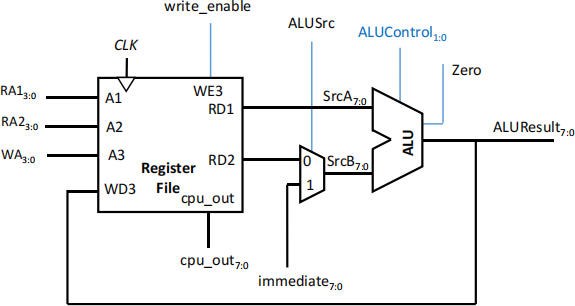
|
Module name |
reg_file_alu |
|
Output ports |
ALUResult[7:0], cpu_out[7:0], Zero |
|
Input ports |
RA1[3:0], RA2[3:0], WA[3:0], immediate[7:0], write_enable, ALUSrc, ALUControl[1:0], CLK |
Write a SystemVerilog module with the name reg_file_alu, implementing the combined ALU and register file as shown above .
Include a 2-to-1 multiplexer, which selects either the RD2 output from the register file, or an external input (immediate) to be input to the ALU input port SrcB.
Write a testbench to simulate the reg_file_alu module, and test it with at least 8 sets of test vectors.
Note that, when the simulation starts, all the registers except x0 will contain 8’hx. To write a value into a register, input the value through the immediate port (ALUSrc = 1), add it to the contents of the register x0 (RA1 = 4’h0, ALUControl = 2’b10) and write the result into the register file (write_enable = 1). [20 marks]
4. Instruction
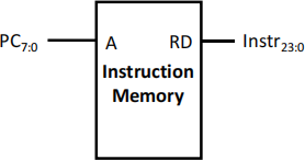
|
Module name |
instruction_memory |
|
Output port |
Instr[23:0] |
|
Input port |
PC[7:0] |
Write a SystemVerilog module, with the name instruction_memory, implementing a read-only memory (ROM) array, storing 256 words of data, with each word being 24 bits wide. Use the example code for the ROM array in the ‘Example SystemVerilog modules’ document.
The output Instr23:0 is asynchronous (it updates instantly whenever the input address is changed). The machine code program to be stored in the ROM is read in from a text file (with the filename ‘program.txt’, saved in the same folder as the SystemVerilog modules) in a single pass behaviour (keyword initial), using the $readmemh system task.
In the text file, list the eight 24-bit values (written as 6-digital hexadecimal numbers) listed in the ‘Machine code program’ column in the table below. This is a machine code program which finds the binary logarithm (log2) of the value stored in register x2, and stores the result in register x15:
|
Instruction memory address |
Machine code program |
Assembly program |
|
|
00 |
610001 |
addi x1, x0, 1 |
# Write the value 1 into register x1 |
|
01 |
620020 |
addi x2, x0, 32 |
# Write the value 32 into x2 |
|
02 |
6F0000 |
addi x15, x0, 0 |
# Write the value 0 into x15 |
|
03 |
701207 |
beq x1, x2, 7 |
# Branch to instruction 7 if x1 == x2 == 32 |
|
04 |
211100 |
add x1, x1, x1 |
# x1 = 2 * x1 |
|
05 |
6FF001 |
addi x15, x15, 1 |
# Increment value in register x15 |
|
06 |
700003 |
beq x0, x0, 3 |
# Unconditional branch to instruction 3 |
|
07 |
700007 |
beq x0, x0, 7 |
# Unconditional branch to instruction 7 |
Write a testbench and test the operation of the ROM module , with 8 input test vectors: PC[7:0] = 8h’00, 8h’01, 8h’02, 8h’03, … 8h’07. Check that each of the machine code instructions is output correctly. [10 marks]
5. Program Counter
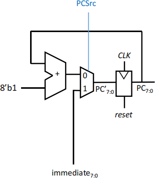
|
Module name |
pc |
|
Output ports |
PC[7:0] |
|
Input ports |
immediate[7:0], PCSrc, CLK, reset |
Implement the 8-bit program counter shown above, as a SystemVerilog module with the name pc. The register should be updated on the positive edges of the clock, and have an active high reset. The 2-to-1 multiplexer selects the next value of PC as either PC+1 (the next instruction in the program will be fetched) or the input immediate (the program branches to an instruction elsewhere).
Write a testbench to test the operation of your program counter module , with at least 8 sets of test vectors. Remember to assert the reset during the first part of the simulation to set the program counter to 0x00 . [10 marks]
6. Combining the ROM with program counter
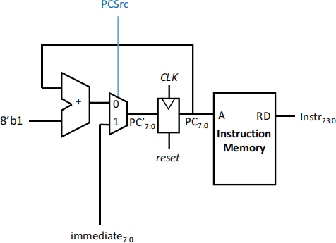
|
Module name |
instruction_memory_pc |
|
Output ports |
Instr[23:0] |
|
Input ports |
immediate[7:0], PCSrc, CLK, reset |
Implement the system shown above, as a SystemVerilog module with the name instruction_memory_pc, combining the ROM array and the counter you wrote in Activities 4 and 5.
Write a testbench to test the operation of the instruction_memory_pc module, ensuring that it correctly outputs all 7 instructions in the memory. Remember to apply a reset at the start of the simulation. [10 marks]![]()
7. Control unit
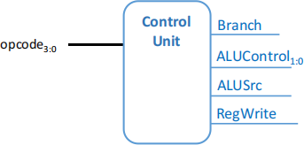
|
Module name |
control_unit |
|
Output ports |
Branch, ALUControl[1:0], ALUSrc, RegWrite |
|
Input ports |
opcode[3:0] |
2023-02-27